
3D nanotomography and nanofabrication tool released by Zeiss
Zeiss will be presenting the first system of the new Crossbeam series at the MC 2013 in Regensburg, Germany.
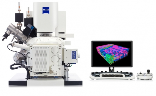
Pictured above, its features include high speed in materials analysis and processing and its wide diversity of applications. Time intensive 3D experiments that used to run for several days can now be completed overnight.
The newly developed focused ion beam (FIB) column enables fast and precise materials processing that can be observed with the field emission scanning electron microscope in real-time. Zeiss points out high resolution over the entire voltage and current range allows users to work quickly and precisely.
The stable system is claimed to provide reproducible results even in long-term experiments. The field of application is expanded by the optionally available Massive Ablation Laser that rapidly prepares samples to access deeply buried regions of interest.
Crossbeam is suitable for use in both materials and life sciences. Materials scientists benefit from the excellent 3D analytics, the ability to image magnetic and non-conductive specimens with maximum resolution, and from the unique material contrasts.
Bioscientists can use Crossbeam, above all, for fast tomography series with high Z resolution in cell and tissue biology. The STEM detection module delivers additional structural information. The system also offers automated workflows.
At the same time, the open software offers users the possibility of integrating and automating their own applications. The modular design of Crossbeam makes it an open 3D nano workstation that can be configured and field-upgraded for a broad spectrum of today's and future applications, therefore offering the user maximum flexibility.
The microscope system is available in two versions. The GEMINI I VP (variable pressure) column of Crossbeam 340 offers optimal analysis conditions for in situ experiments with outgassing and charging specimens.
Thanks to the GEMINI II column with double condenser system, Crossbeam 540 users benefit from more information in a shorter time. The system delivers high resolution, even with low voltage and high beam current, enabling fast analytics and ease of use.
In combination with a Zeiss Xradia X-ray microscope (XRM), Crossbeam offers the possibility of complete specimen analysis across several orders of magnitude. The X-ray microscope first provides a 3D image of the specimen without destroying it before the identified areas of interest are processed with the focused ion beam and analyzed with the electron beam.


