
Dow and EVG to enhance temporary bonding for 3D-ICs
Both innovators are uniting to offer simple, cost-effective temporary bonding/debonding solution for high-performance 3D-IC packaging
Dow Corning has joined EV Group's network of technology providers to support EVG's LowTemp platform for room-temperature wafer bonding and debonding processes.
The addition of Dow Corning - a specialist in silicon-based technology, silicones, and innovation - to EVG's list of collaboration partners follows intensive co-development efforts between the two companies, including stringent testing of Dow Corning's simple and innovative bi-layer temporary bonding technology.
EVG launched its new open LowTemp platform in July when it also announced the expansion of its global materials supply chain to accelerate the growth of high-end 3D-IC packaging.
"As a global leader in advanced silicone technology and expertise, Dow Corning is an important and much welcomed addition to our open temporary wafer bonding/debonding materials platform," says Thorsten Matthias, business development director, EV Group.
"Their collaborative approach and exceptional materials expertise helped us to develop an innovative, cost-effective temporary bonding solution that now offers our customers expanded options for room-temperature bonding and debonding of active and carrier wafers using conventional manufacturing methods."
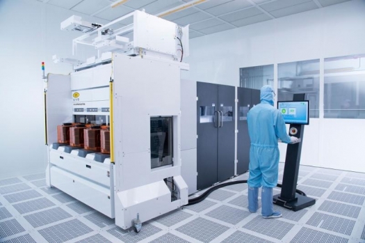
EVG's LowTemp temporary bonding/debonding platform (TB/DB) features three different room-temperature wafer-debonding processes - ultraviolet (UV) laser debonding, multilayer adhesive debonding and ZoneBOND technology - that have been qualified for the company's high-volume production.
Dow Corning's bi-layer TB/DB silicone technology is a natural fit for the EVG platform in that it comprises an adhesive and release layer that enables simple, room-temperature TB/DB, and delivers best-in-class performance with regard to low total thickness variation. It also provides excellent chemical resistance and good thermal stability when exposed to temperatures reaching 3000 C.
By assigning Dow Corning qualified supplier status for its open materials platform, EVG significantly strengthens and expands the global supply chain for its world-class TB/DB technologies. Through this non-exclusive agreement, the two companies now offer the advanced semiconductor packaging industry a cost-effective TB/DB solution to support high-volume production of 3D-IC packaging applications.
"This collaboration signifies another major milestone for Dow Corning, EVG and the semiconductor industry as a whole with regard to 3D IC and through silicon via development," says Andrew Ho, global industry director, Advanced Semiconductor Materials at Dow Corning.
He continues, "In addition to signalling another important validation of Dow Corning's simple, room-temperature temporary bonding/debonding technology, it enables further commercialisation of EVG's leading-edge open platform for volume manufacturing. Equally important, this technology represents a major step forward toward the further integration of the 3D-IC packaging process for next-generation microelectronic applications."
3D-IC integration promises to significantly improve the form factor, bandwidth and functionality of microelectronic devices by enabling once-horizontal chip structures to be fabricated into vertical architectures.
However, this revolutionary new technology first requires simple, cost-effective TB/DB solutions to adhere active device wafers to thicker carrier wafers. This allows subsequent thinning of the active wafer down to 50 µm or less, and fabrication of through-silicon vias that enable vertical interchip communication.
EVG will showcase its latest developments in wafer bonding and other processing solutions at the company's booth #416 in the TWTC Nangang Exhibition Hall at the SEMICON Taiwan.
Also, Markus Wimplinger, corporate technology development and IP director at EV Group, will present a paper entitled "Cost Effective Thin Wafer Handling with LowTemp Debonding" at SEMICON Taiwan's TechXPOT on September 4th from 15:30 to 16:00. Wimplinger will also present "Trends in Wafer Bonding for High Volume Consumer MEMS Applications," at the show's MEMS Forum on September 5th from 15:10 to 15:40.


