
News Article
Rudolph expands macro defect inspection series
The new NSX 220 tool is designed for semiconductor, MEMS and LED packaging and test facilities to achieve productivity at a low price
Rudolph Technologies has launched its new NSX 220 automated macro defect inspection system.
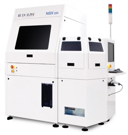
The company says its system, pictured below, provides fast, easy defect inspection for traditional back-end processes including the LED market at a reduced price.

NSX220 system
The NSX 220 tool joins the NSX 320 system in the NSX family of automated macro defect inspection and metrology systems for final manufacturing facilities.
The first NSX 220 system was installed in July at a major outsourced assembly and test (OSAT) facility in Asia.
Mike Jost, vice president and general manager of Rudolph’s Inspection Business Unit says, “The NSX 220 system is a streamlined version of our NSX 320 system. The NSX 220 system is designed for traditional macro defect inspection of wafers up to 300mm at conventional semiconductor, MEMS and LED final manufacturing facilities, while the NSX 320 System serves next-generation advanced packaging processes with defect inspection and three-dimensional metrology for wafers up to 450mm."
He continues, "The NSX 220 system benefits from many of the hardware and software innovations that made the NSX 320 system the market leader in advanced packaging, but is targeted for back-end facilities that do not need the full suite of capabilities offered by the NSX 320 System. Adding the NSX 220 system to the NSX family gives our customers a choice of best-in-class capabilities.”
The NSX 220 is an automated macro defect inspection system that uses grey-scale image analysis (with colour image capture) to provide fast, accurate inspection and metrology in final manufacturing applications for wafers up to 300mm. It can detect traditional advanced macro defects such as scratches, mechanical damage, foreign materials, voids and probe damage, while also performing two-dimensional measurements on bumps, probe marks and edge trim processes.
The tool operates over a range of resolutions (10µm - 0.5µm) with both brightfield and optional darkfield illumination. The software platform, leveraged from the NSX 320 system’s success, uses host-based image processing and delivers significant improvements in usability and productivity over older-generation NSX series equipment. Using centrally-managed recipe creation and editing, multiple NSX 220 tools can share a single recipe and be matched across the fab.
An optional suite of yield management software optimises the productivity of both the NSX 220 and 320 systems and minimises the need for operator assistance. Discover Software is designed for use with Rudolph inspection systems to allow real-time analysis for faster solutions and intelligent defect sampling for reduced offline review.
Rudolph will provide more information on its NSX 220 inspection system at SEMICON Taiwan taking place from September 4th to 6th, 2013.
The company says its system, pictured below, provides fast, easy defect inspection for traditional back-end processes including the LED market at a reduced price.
NSX220 system
The NSX 220 tool joins the NSX 320 system in the NSX family of automated macro defect inspection and metrology systems for final manufacturing facilities.
The first NSX 220 system was installed in July at a major outsourced assembly and test (OSAT) facility in Asia.
Mike Jost, vice president and general manager of Rudolph’s Inspection Business Unit says, “The NSX 220 system is a streamlined version of our NSX 320 system. The NSX 220 system is designed for traditional macro defect inspection of wafers up to 300mm at conventional semiconductor, MEMS and LED final manufacturing facilities, while the NSX 320 System serves next-generation advanced packaging processes with defect inspection and three-dimensional metrology for wafers up to 450mm."
He continues, "The NSX 220 system benefits from many of the hardware and software innovations that made the NSX 320 system the market leader in advanced packaging, but is targeted for back-end facilities that do not need the full suite of capabilities offered by the NSX 320 System. Adding the NSX 220 system to the NSX family gives our customers a choice of best-in-class capabilities.”
The NSX 220 is an automated macro defect inspection system that uses grey-scale image analysis (with colour image capture) to provide fast, accurate inspection and metrology in final manufacturing applications for wafers up to 300mm. It can detect traditional advanced macro defects such as scratches, mechanical damage, foreign materials, voids and probe damage, while also performing two-dimensional measurements on bumps, probe marks and edge trim processes.
The tool operates over a range of resolutions (10µm - 0.5µm) with both brightfield and optional darkfield illumination. The software platform, leveraged from the NSX 320 system’s success, uses host-based image processing and delivers significant improvements in usability and productivity over older-generation NSX series equipment. Using centrally-managed recipe creation and editing, multiple NSX 220 tools can share a single recipe and be matched across the fab.
An optional suite of yield management software optimises the productivity of both the NSX 220 and 320 systems and minimises the need for operator assistance. Discover Software is designed for use with Rudolph inspection systems to allow real-time analysis for faster solutions and intelligent defect sampling for reduced offline review.
Rudolph will provide more information on its NSX 220 inspection system at SEMICON Taiwan taking place from September 4th to 6th, 2013.


