+44 (0)24 7671 8970
More publications     •     Advertise with us     •     Contact us
 
News Article

SEMI: Flash market to increase by a massive 40 percent

News

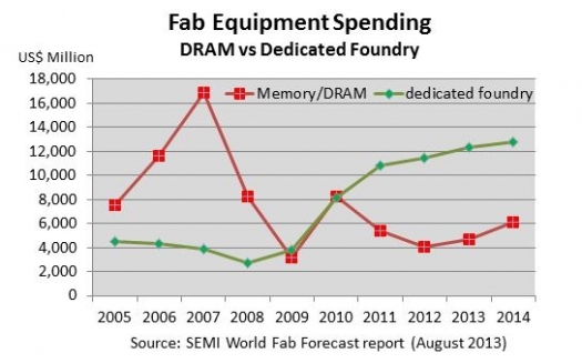
While DRAM equipment spending dropped by 35 percent in 2011 and 25 percent in 2012, SEMI says its data shows that DRAM fab equipment spending will increase by 17 percent in 2013 and at least 30 percent in 2014.

An increase of about 2 to 3 percent for installed capacity for DRAM in 2014 is small but remarkable, given that the industry has not added any new DRAM capacity for years, and actually cutback capacity between 2011 and 2013.

The sector with largest growth rate for fab equipment spending in 2014 is expected to be Flash with a 40 to 45 percent increase (YoY). Over the last few years, capacity additions for the Flash sector also stagnated though technology investments. SEMI's reports show detailed predictions for robust spending in DRAM and Flash by several large companies including Micron and Samsung.

Overall fab equipment spending for Flash alone is expected to hit a record of almost $8 billion in 2014. After Flash and DRAM, MPU is expected to show the next largest growth in 2014, with fab equipment spending growing by over 40 percent (YoY). Intel is now preparing for 14nm, kicking off an MPU surge for 2014.

Since the last fab database publication at the end May 2013, the SEMI worldwide dedicated analysis team has made 242 updates to 205 facilities (including Opto/LED fabs) in the database. The latest edition of the World Fab Forecast lists 1,147 facilities (including 247 Opto/LED facilities), with 66 facilities with various probabilities starting production this year and in the near future. SEMI added 14 new facilities and closed 8 facilities.


Purdue, imec, Indiana announce partnership
Resilinc partners with SEMI on supply chain resilience
NIO and NXP collaborate on 4D imaging radar deployment
Panasonic Industry digitally transforms with Blue Yonder
Global semiconductor sales decrease 8.7%
MIT engineers “grow” atomically thin transistors on top of computer chips
Keysight joins TSMC Open Innovation Platform 3DFabric Alliance
Leti Innovation Days to explore microelectronics’ transformational role
Quantum expansion
indie launches 'breakthrough' 120 GHz radar transceiver
Wafer fab equipment - facing uncertain times?
Renesas expands focus on India
Neuralink selects Takano Wafer Particle Measurement System
Micron reveals committee members
Avoiding unscheduled downtime in with Preventive Vacuum Service
NFC chip market size to surpass US$ 7.6 billion
Fujifilm breaks ground on new €30 million European expansion
Fraunhofer IIS/EAS selects Achronix embedded FPGAs
Siemens announces certifications for TSMC’s latest processes
EU Chips Act triggers further €7.4bn investment
ASE recognised for excellence by Texas Instruments
Atomera signs license agreement with STMicroelectronics
Gartner forecasts worldwide semiconductor revenue to decline 11% in 2023
CHIPS for America outlines vision for the National Semiconductor Technology Center
TSMC showcases new technology developments
Alphawave Semi showcases 3nm connectivity solutions
Greene Tweed to open new facility in Korea
Infineon enables next-generation automotive E/E architectures
Global AFM market to reach $861.5 million
Cepton expands proprietary chipset
Semtech adds two industry veterans to board of directors
Specialty gas expansion
×
Search the news archive

To close this popup you can press escape or click the close icon.
Logo
×
Logo
×
Register - Step 1

You may choose to subscribe to the Silicon Semiconductor Magazine, the Silicon Semiconductor Newsletter, or both. You may also request additional information if required, before submitting your application.


Please subscribe me to:


You chose the industry type of "Other"

Please enter the industry that you work in: