
New ink-jet technology can lead to new classes of electronics
A multi-institutional team of engineers has developed a new approach to the fabrication of nanostructures for the semiconductor and magnetic storage industries.
This approach combines top-down advanced ink-jet printing technology with a bottom-up approach that involves self-assembling block copolymers, a type of material that can spontaneously form ultrafine structures.
The team, consisting of nine researchers from the University of Illinois at Urbana-Champaign, the University of Chicago and Hanyang University in Korea, was able to increase the resolution of their intricate structure fabrication from approximately 200 nanometres (nm) to approximately 15nm. A nanometre, a billionth of a metre is the width of a double-stranded DNA molecule.
The ability to fabricate nanostructures out of polymers, DNA, proteins and other "soft" materials has the potential to enable new classes of electronics, diagnostic devices and chemical sensors. The challenge is that many of these materials are fundamentally incompatible with the sorts of lithographic techniques that are traditionally used in the integrated circuit industry.
Recently developed ultrahigh resolution ink-jet printing techniques have some potential, with demonstrated resolution down to 100 to 200nm, but there are significant challenges in achieving true nanoscale dimension. "Our work demonstrates that processes of polymer self-assembly can provide a way around this limitation," says John Rogers, the Swanlund Chair Professor in Materials Science and Engineering at Illinois.
Rogers and his associates report their findings in the September issue of Nature Nanotechnology. Combining jet printing with self-assembling block copolymers enabled the engineers to attain the much higher resolution, as suggested by lead author Serdar Onses, a postdoctoral scientist at Illinois.
Onses earned his doctorate at the University of Wisconsin under Paul Nealey, now the Brady W. Dougan Professor in Molecular Engineering at UChicago and a co-author of the Nature Nanotechnology paper. "This concept turned out to be really useful," Rogers says.
Engineers use self-assembling materials to augment traditional photolithographic processes that generate patterns for many technological applications. They first create either a topographical or chemical pattern using traditional processes. For the Nature Nanotechnology paper, this was done at imec in Belgium, an independent nanoelectronics research centre. Nealey's laboratory pioneered this process of directed self-assembly of block copolymers using chemical nanopatterns.

A technician sits at a track system at imec. The system coats, bakes and develops thin polymer films on silicon wafers. They are critical steps in the fabrication of samples that imec provides to Paul Nealey's research group at the University of Chicago's Institute for Molecular Engineering
Nearing the limits
The resolution of the chemical pattern nears the current limit of traditional photolithography, notes Lance Williamson, a graduate student in molecular engineering at UChicago and co-author of the Nature Nanotechnology article. "Imec has the capability to perform the photolithography at this scale over large areas with high precision," Williamson comments.
Back at the University of Illinois, engineers place a block copolymer atop this pattern. The block copolymer self-organises, directed by the underlying template to form patterns that are at much higher resolution than the template itself.
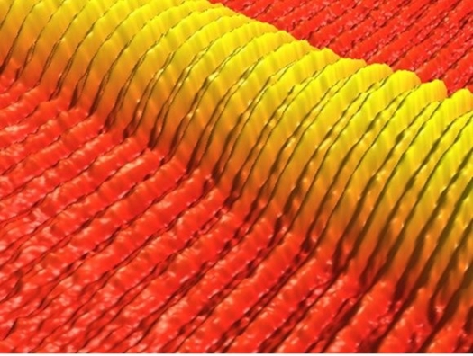
The atomic force microscope image at the top of this story shows directed self-assembly of a printed line of block copolymer on a template prepared by photolithography. The microscope's software coloured and scaled the image. The density of patterns in the template (bounded by the thin lines) is two times that of the self-assembled structures (the ribbons).
Previous work has focused on the deposition and assembly of uniform films on each wafer or substrate, resulting in patterns with essentially only one characteristic feature size and spacing between features. But practical applications may need block copolymers of multiple dimensions patterned or spatially placed over a wafer.
"This invention, to use inkjet printing to deposit different block copolymer films with high spatial resolution over the substrate, is highly enabling in terms of device design and manufacturing in that you can realise different dimension structures all in one layer," Nealey says. "Moreover, the different dimension patterns may actually be directed to assemble with either the same or different templates in different regions."
Benefits of e-jet printing
The advanced form of ink-jet printing the engineers use to locally deposit block copolymers is called electrohydrodynamic, or e-jet printing. It operates much like the ink-jet printers office workers use for printing on paper.
"The idea is flow of materials from small openings, except e-jet is a special, high-resolution version of ink-jet printers that can print features down to several hundred nanometres," Onses says. And because e-jet can naturally handle fluid inks, it is exceptionally well-suited for patterning solution suspensions of nanotubes, nanocrystals, nanowires and other types of nanomaterials.
"The most interesting aspect of this work is the ability to combine "˜top-down' techniques of jet printing with "˜bottom-up' processes of self-assembly, in a way that opens up new capabilities in lithography - applicable to soft and hard materials alike," Rogers notes.
"The opportunities are in forming patterned structures of nanomaterials to enable their integration into real devices. I am optimistic about the possibilities."
Details of this work have been published in the paper, "Hierarchical patterns of three-dimensional block-copolymer films formed by electrohydrodynamic jet printing and self-assembly," by M. Serdar Onses et al in Nature Nanotechnology, September 2013, pages 667-675.
This work was funded by the National Science Foundation and National Research Foundation of Korea.


