
Integrating graphene photodetectors into silicon chips
The novel material graphene and its technological applications are being studied at the Vienna University of Technology. Now scientists have succeeded in combining graphene light detectors with semiconductor chips
Today, most information is transmitted by light - for example in optical fibres. Computer chips, however, work electronically. Somewhere between the optical data highway and the electronic chips, photons have to be converted into electrons using light-detectors.
Scientists at the Vienna University of Technology have now managed to combine a graphene photodetector with a standard silicon chip. It can transform light of all important frequencies used in telecommunications into electrical signals. The scientific results have now been published in the journal Nature Photonics.
Computing Power Made of Carbon?
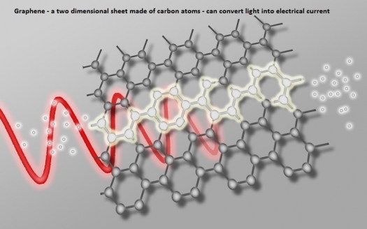
Both academia and the industry have high hopes for graphene. The material, which consists of a single layer of hexagonally arranged carbon atoms, has extraordinary properties. Two years ago, the team around Thomas Mueller (Institute of Photonics, Vienna University of Technology) demonstrated that graphene is ideally suited to turn light into electrical current.
"There are many materials that can transform light into electrical signals, but graphene allows for a particularly fast conversion", says Thomas Mueller. So wherever large amounts of data are to be transmitted in a short period of time, graphene will in the future probably be the material of choice.
The researchers had to come a long way from the basic proof of what the material can do to actually using it in a chip - now they have succeeded. The Viennese team worked together with researchers from the Johannes Kepler University in Linz.
"A narrow waveguide with a diameter of about 200 by 500 nanometres carries the optical signal to the graphene layer. There, the light is converted into an electrical signal, which can then be processed in the chip", Thomas Mueller explains.

Image showing the light signal arriving through a waveguide (left), in the 2 micrometre wide graphene sheet, where electrical current is generated
Versatile and Compact
There have already been attempts to integrate photodetectors made of other materials (such as germanium) directly into a chip. However, these materials can only process light of a specific wavelength range. The researchers were able to show that graphene can convert all wavelengths which are used in telecommunications equally well.
The graphene photodetector is not only extremely fast, it can also be built in a particularly compact way. 20 000 detectors can fit onto a single chip with a surface area of one square centimetre. Theoretically, the chip could be supplied with data via 20 000 different information channels.
More Speed, Less Energy
"These technologies are not only important for transmitting data over large distances. Optical data transmission also becomes more and more important within computers themselves", says Thomas Mueller.
When large computer clusters work with many processor cores at the same time, a lot of information has to be transferred between the cores. As graphene allows switching between optical and electrical signals very quickly, this data can be exchanged optically. This speeds up the data exchange and requires much less electrical energy.
This work is described in detail in the paper, "CMOS-compatible graphene photodetector covering all optical communication bands," by Andreas Pospischil et al in Nature Photonics, (2013)., published online on 15th September 2013. doi:10.1038/nphoton.2013.240


