
News Article
Renesas reveals advanced low-power SRAM devices
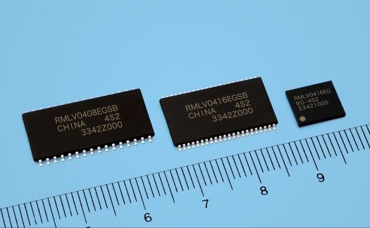
Renesas Electronics Corporation has introduced 12 new product versions in the RMLV0416E, RMLV0414E, and RMLV0408E series of Advanced Low-Power SRAM (Advanced LP SRAM), the company's flagship SRAM (static random access memory) devices.
The new memory devices have a density of 4 megabits (Mb) and utilise a fine fabrication process technology with a circuit line-width of 110 nanometres (nm).
The forthcoming SRAMs are the new series of Advanced LPSRAM and provide high reliability equivalent to that of Renesas' existing SRAM products adopting a 150 nm process, including soft error1 free and latch-up2 free. They also achieve low-power operation with a standby current of maximum of 2 microamperes (µA) at 25°C, making them suitable for data storage in battery-backup devices.
According to Renesas, its low-power SRAMs have achieved widespread adoption in many different fields, including industrial, office, communication, automotive, and consumer products and the company held the #1 market share worldwide in such products in 2012.
Recently, as manufacturers systems have attained higher performance and more advanced functionality, SRAM has become an important factor in improving overall system reliability. In particular, SRAM used to store important information such as system programs and billing data must provide a high level of reliability, and particular attention has come to be focused on measures to reduce soft error caused by alpha radiation and cosmic neutron radiation.
Renesas' Advanced LP SRAM has structure in which each memory node3 within the memory cells hast an added physical capacitor, resulting in extremely high endurance against soft error.
A general method of dealing with soft error after they occur is the inclusion of an internal error correcting code (ECC) circuit in the SRAM or the manufacturer systems. This approach has its limits, however, and there may be cases where the performance of the ECC is unable to deal with errors affecting multiple bits.
In contrast, Advanced LP SRAMs use structural measures to prevent the soft error themselves from occurring. Results from the evaluation of system soft error in 150 nm Advanced LP SRAMs that are currently in mass production prove that, in practical terms, these products can be called soft error free.
In addition, the SRAM cell load transistors (p-channels) are polysilicon TFTs4 and they are stacked on top of the n-channel MOS transistors on the silicon substrate. Therefore, only the n-channel transistors are formed below on the silicon substrate. This ensures that no parasitic thyristors can form within the memory area and theoretically makes latchups impossible.
These features enable Advanced LP SRAMs to achieve far higher levels of reliability than full CMOS-type5 products using a conventional memory cell structure. Advanced LP SRAMs can contribute to even better performance and reliability in applications where a high level of reliability is essential, such as factory automation equipment, measuring devices, equipment employed in smart grids, and transportation systems.
What's more, Advanced LP SRAM combines SRAM polysilicon TFT stacking technology and stacked capacitor6 technology to reduce the cell size. For example, the cell size of 110 nm Advanced LP SRAM is comparable to that of full CMOS SRAM fabricated using a 65 nm process.
Renesas intends to strengthen its lineup of 110 nm SRAMs by adding 8 Mb and 64 Mb 110 nm products.
Pricing and Availability Samples of Renesas Electronics' new SRAMs will be available in November 2013, priced at US$7.0. Mass production is scheduled to begin in December 2013. (Pricing and availability are subject to change without notice.)
1 Soft error: A phenomenon in which an electric charge is generated when external alpha or neutron radiation strikes the silicon substrate, causing the data stored in the memory to be lost. In contrast to hard error such as physical failures in semiconductor elements, which are reproducible, soft error is not reproducible and can be corrected simply by having the system rewrite the data. Generally speaking, the rate of soft error increases as the fabrication process becomes finer.
2 Latchup: A phenomenon in which an npn or pnp structure (parasitic bipolar transistor) formed by the well, silicon substrate, P-type diffusion layer, and n-type diffusion layer of a CMOS transistor enters the on state due to overvoltage from the power supply or input pins, allowing a large current to flow between the power supply and ground.
3 Memory nodes: Flip-flop circuit nodes within each memory cell that store bits of information as "high" or "low" electric potential.
4 Thin-film transistor (TFT): A transistor generated from thin-film polysilicon. Such elements are used as the SRAM load transistors, generated on the top layer of the MOS transistors on the silicon substrate to effectively reduce the surface area of the memory cells.
5 Full CMOS type: An SRAM memory cell structure composed of a total of six P-channel MOS transistors and N-channel MOS transistors generated on the same silicon substrate surface. It has a large surface area and there is a risk of latchups.
6 Stacked capacitors: Capacitors with two electrodes generated from polysilicon or metal. These capacitors are generated on the upper layer of the MOS transistors on the silicon substrate to effectively reduce the surface area of the memory cell.


