Silicon interposers: has the market arrived?

Traditionally the chip packaging community defines an interposer as the bridge between the on chip pitch and the on board pitch. In other words, the interposer is traditionally the package. With 2.5D or 3D, once again it's all about the pitch. Chip IO cannot be connected in a stack unless the interfaces have been standardised to match.
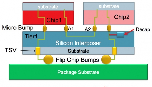
So todays 2.5D interposer serves as a high density RDL (Redistribution Layer) so the chips can be connected either through the interposer, such as Elpida's stacked memory or next to each other on the interposer such as the Xilinx FPGA .The latter structure bears a strong resemblance to the MCM-D (Deposited-Multi Chip Module) of the 1990's. The one criteria true for all of todays 2.5D interposers is that they must contain TSV (Through Silicon Via).
Silicon interposers appear on company roadmaps for networking products and servers and for applications including GPUs (Graphics Processing Units) and sensors. Stacked memory that can be mounted on the interposer next to the logic device is required for networking applications and adoption depends on the availability from key memory suppliers.
TechSearch International, Inc. has released its analysis of the market for silicon interposers. The report highlights the latest trends in silicon interposer supply and demand.
TSMC has been the main supplier of fine feature size silicon interposers, but other suppliers are coming on line and production is scheduled to ramp. The cost of the interposer is a concern for some applications and alternatives such as organic or glass interposers are being examined. Several alternative packaging configurations are also planned.


