
News Article
Enhancing amorphous silicon quantum dots
Simulations have helped North and South Dakota researchers decide which technology would make a better solar collector, quantum dot or nanowire
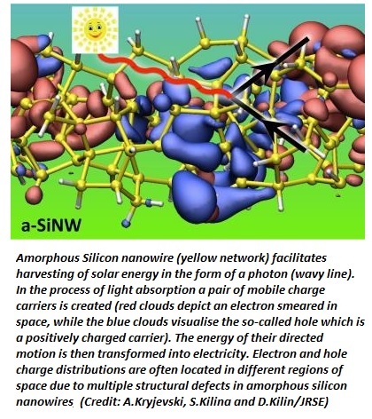
A trio of researchers at North Dakota State University and the University of South Dakota have turned to computer modelling to help decide which of two competing materials should get its day in the sun as the nanoscale energy-harvesting technology of future solar panels - quantum dots or nanowires. Andrei Kryjevski and his colleagues, Dimitri Kilin and Svetlana Kilina, report in AIP Publishing's Journal of Renewable and Sustainable Energy that they used computational chemistry models to predict the electronic and optical properties of three types of nanoscale (billionth of a metre) silicon structures with a potential application for solar energy collection: a quantum dot, one-dimensional chains of quantum dots and a nanowire. The ability to absorb light is substantially enhanced in nanomaterials compared to those used in conventional semiconductors. Determining which form - quantum dots or nanowire - maximises this advantage was the goal of the numerical experiment conducted by the three researchers. "We used Density Functional Theory, a computational approach that allows us to predict electronic and optical properties that reflect how well the nanoparticles can absorb light, and how that effectiveness is affected by the interaction between quantum dots and the disorder in their structures," Kryjevski says. "This way, we can predict how quantum dots, quantum dot chains and nanowires will behave in real life even before they are synthesised and their working properties experimentally checked." The simulations made by Kryjevski, Kilin and Kilina indicated that light absorption by silicon quantum dot chains significantly increases with increased interactions between the individual nanospheres in the chain. They also found that light absorption by quantum dot chains and nanowires depends strongly on how the structure is aligned in relation to the direction of the photons striking it. Finally, the researchers learned that the atomic structure disorder in the amorphous nanoparticles results in better light absorption at lower energies compared to crystalline-based nanomaterials. "Based on our findings, we believe that putting the amorphous quantum dots in an array or merging them into a nanowire are the best assemblies for maximising the efficiency of silicon nanomaterials to absorb light and transport charge throughout a photovoltaic system," Kryjevski said. "However, our study is only a first step in a comprehensive computational investigation of the properties of semiconductor quantum dot assemblies. "The next steps are to build more realistic models, such as larger quantum dots with their surfaces covered by organic ligands and simulate the processes that occur in actual solar cells," he adds. Further details of this work have been published in the paper, "Amorphous silicon nanomaterials: Quantum dots versus nanowires," by Andrei Kryjevski et al in Applied Physics Letters, Journal of Renewable and Sustainable Energy 5, 043120 (2013); http://dx.doi.org/10.1063/1.4817728


