
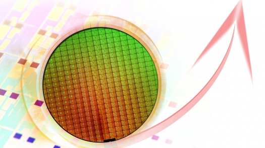
Noel Technologies offers 450mm wafer services
The Silicon Valley specialty foundry will initially offer semiconductor wet processes, etches and cleans, and resist spin coatings and films
Noel Technologies has increased its capabilities by offering 450mm wafer services.
Noel now jumps into the R&D transition to the larger wafer size as toolmakers and customers prepare for the 450mm generation.
The specialty foundry will first offer services for 450mm wafers in wet processes, etches, and wafer cleaning. Later this year, they will add photoresist spin coatings and in 2014 plans include adding LPCVD nitride & LPCVD undoped poly films.
"We wanted to be at the essential leading edge of the transition to the next wafer size," comments Noel Technologies Founder and CTO Leon Pearce. "We will start by putting in the R&D foundation and offering several coating, cleaning and films processes. We realise this transition may take time and that the larger size offers challenges to manufacturers and foundries alike, including handling, cleanliness and creative process solutions. We're dedicated to learning to process 450mm wafers along with our customers as they trend toward that transition."
Noel Technologies is focused on process development, optimisation, quality and delivery. An ISO 9001 registered facility, Noel Technologies offers process development and fabrication now up to 450mm.
As the increasing costs of technology R&D, along with slower revenue growth, continue to drive the expansion of the fabless model, Noel Technologies is strategically positioned to provide IDMs with a bridge from lab to fab.


