
Quantitative nanoscopic imaging possible through silicon
The new technology, which relies on near-infrared light, could help scientists learn more about diseased or infected cells as they flow through silicon microfluidic devices.
"This has the potential to merge research in cellular visualisation with all the exciting things you can do on a silicon wafer," says Ishan Barman, a former postdoctoral researcher in MIT's Laser Biomedical Research Center (LBRC) and one of the lead authors of a paper describing the technology in Scientific Reports.
Silicon is commonly used to build "lab-on-a-chip" microfluidic devices, which can sort and analyse cells based on their molecular properties, as well as microelectronics devices.
Such devices have many potential applications in research and diagnostics, but they could be even more useful if scientists could image the cells inside the devices, says Barman, who is now an assistant professor of mechanical engineering at Johns Hopkins University.
To achieve that, Barman and colleagues took advantage of the fact that silicon is transparent to infrared and near-infrared wavelengths of light. They adapted a microscopy technique known as quantitative phase imaging, which works by sending a laser beam through a sample, then splitting the beam into two. By recombining those two beams and comparing the information carried by each one, the researchers can determine the sample's height and its refractive index.
Traditional quantitative phase imaging uses a helium neon laser, which produces visible light, but for the new system the researchers used a titanium sapphire laser that can be tuned to infrared and near-infrared wavelengths. For this study, the researchers found that light with a wavelength of 980 nm worked best.
Using this system, the researchers measured changes in the height of red blood cells, with nanoscale sensitivity, through a silicon wafer similar to those used in most electronics laboratories.
As red blood cells flow through the body, they often have to squeeze through very narrow vessels. When these cells are infected with malaria, they lose this ability to deform, and form clogs in tiny vessels. The new microscopy technique could help scientists study how this happens, Dingari says; it could also be used to study the dynamics of the malformed blood cells that cause sickle cell anaemia.
The team overcame past limitations on quantitative microscopy through an opaque media by working with a new combination of near infrared light and a technique called quantitative phase imaging. Quantitative phase imaging is about a decade old. It uses shifts in phases of light, not staining techniques, to aid specimen imaging - earning the term "label-free."
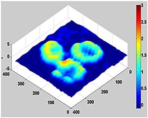
The image at the top of this story shows a quantitative phase image of red blood cells. The image is courtesy of the researchers.
The researchers also used their new system to monitor human embryonic kidney cells as pure water was added to their environment - a shock that forces the cells to absorb water and swell up. The researchers were able to measure how much the cells distended and calculate the change in their index of refraction.
"Nobody has shown this kind of microscopy of cellular structures before through a silicon substrate," Mohanty, a UTA researcher says.
Mohanty's laboratory at UTA is now using the system to study how neurons grown on a silicon wafer communicate with each other.
The researchers used silicon wafers that were about 150 to 200 µm thick, but they have since shown that thicker silicon can be used if the wavelength of light is increased into the infrared range. The researchers are also working on modifying the system so that it can image in three dimensions, similar to a CT scan.
The new paper which details this work is called, "Label-free route to rapid, nanoscale characterization of cellular structure and dynamics through opaque media," by Bipin Joshi et al in Scientific Reports 3, 2822. It is available online here: http://www.nature.com/srep/2013/131002/srep02822/full/srep02822.html Mohanty's group has recently combined the near infrared quantitative phase imaging with near-infrared optical tweezers for tomographic imaging of cells which is described in the paper, "Optical tweezers assisted quantitative phase imaging led to thickness mapping of red blood cells", by N. Cardenas et al in Applied Physics Letters, 103, 013703 (2013). The joint UT Arlington/ MIT research was supported by Nanoscope Technologies and funded in part by a National Institute of Biomedical Imaging and Bioengineering grant.


