
ADEKA'S additive for copper plating ideal for TSV filling
In recent times, semiconductor manufacturers have been attempting to achieve a smaller size and improve the performance of devices by stacking multiple chips into a 3D structure.
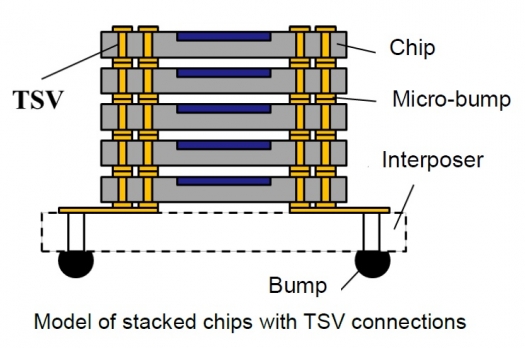
Considering the benefits of the shortest and high-density connections, Through Silicon Via (TSV) technology has been indispensable in creating these 3D structures.
TSV electrodes provide vertical electrical connections that pass internally through semiconductor chips. This is shown in the schematic at the top of this story.
Now Tokyo headquartered firm ADEKA Corporation has developed a new single-component type additive for TSV copper plating. The versatile material should reduce costs and defects.
The TSV copper plating materials field is anticipated to be a 10 billion yen (¥) market (or roughly US $ 0.1 billion) from 2017, where additives will occupy around ¥5 billion.
ADEKA aims to acquire a market share of 50 percent by establishing the new additive system.
Development of TSV-based 3D structures involves key technologies such as the formation of via (a small hole a few micrometres to a few tens of micrometres in diameter) and via filling with conductors. The via filling technique based on copper electroplating is one of the most important technologies for electrode formation.
In the copper filling process, TSV must be perfectly filled without voids or seams for a reliable electrical connection. The copper sulphate plating solution for copper plating contains a suitable balance of several types of additives (such as the accelerator, suppressor, and leveller).
ADEKA says its newly developed additive is of a single type and gives high performance with the copper filling.
The features of this new additive include the following:
(1) Single component enhances manageability:
Strict constant control of plating solutions is required at manufacturing sites that use plating methods. This new single-component type additive makes it easier to control solutions compared with other types, leading to a significant cost reduction.
(2) Complete bottom-up filling:
Bottom-up filling (copper deposition progress from the bottom of the via) avoids the occurrence of defects in the filled copper as shown in the figure below.

Cross-sectional SEM images of plated TSV 1 (Via filling with the new additive)
(3) Highly versatile:
The new additive is effective with TSVs of various sizes. We confirmed perfect filling for a wide range of via sizes, i.e. 5 to 20 micrometres in diameter and aspect ratios of 1 to 10. The additive is also effective with via holes of different sizes on the same wafer. This is shown in the micrograph below.

Cross-sectional SEM image of plated TSV 2 (Simultaneous filling of different sizes with the new additive)


