
News Article
Bringing silicon closer to photons
Researchers have made light move through a 2D landscape consisting of nearly flat ring-shaped silicon waveguides. This could one day aid in the miniaturisation of optical communication devices
Topology, the understanding of how things are connected, remains abstract, even with the well known example of doughnuts and coffee cups. This concept, mysterious as it may seem, is also cool because it is the basis for creating ultrastable quantum "playgrounds." In topological systems, certain quantum behaviours can be carefully probed and harnessed for all kinds of practical applications - from metrology to electronics. Topological insulators, for instance, have garnered attention because they exhibit quantum Hall physics practically off-the-shelf - without the fuss of stringent laboratory conditions. More recently, scientists have sought to go beyond these exotic materials, by designing devices whose topological features can be tuned, or even generated on-demand, like a switch. Quantum Hall physics, inherently topological, has been seen in electronic devices and in dilute atomic ensembles. In the two-dimensional electron case, current flows along an edge/interface ("edge states") even in the presence of defects or other physical distortions in the sample - this arises from global properties of the material. This is strange when contrasted with conventional conductors / insulators, where the transport is impeded due the presence of disorder. In this week's issue of Nature Photonics, scientists at the Joint Quantum Institute (JQI) report what they say is the first observation of such topological effects for light in two dimensions. To accomplish this, they built a structure to guide infrared light over the surface of a room temperature, this.
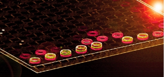
To accomplish this, they built a structure to guide infrared light over the surface of a room temperature, silicon-on-insulator (SOI) chip. Amazingly, they directly observed light racing around the boundary, impervious to defects. The researchers say these photonic edge states are directly analogous to the quantum Hall effect for electrons. The image at the top of this story shows an artistic rendering of real data and real SEM image (false coloured) from experiment. The lit resonators show light racing around the edge of the silicon chip unimpeded, avoiding defects (here a missing resonator). (Credit: E. Edwards/JQI. Figure attributes (colour, lighting) altered for artistic purposes with permission of authors.) Since silicon is the preferred material for most electronics this novel design assists with the miniaturisation of optical communication technology, bringing photons a little closer to their electronic circuit counterparts. The work is a realisation of a theoretical proposal by this same group of JQI scientists and their collaborators more than a year ago. Edge States and Ring Resonators Electrons can occupy topological edge states because they are charged particles whose energy spectrum can be dramatically modified by large magnetic fields. To simplify this, a magnetic interaction is key for realising quantum Hall states. The question here is how the researchers can design a material where photons - massless, charge-free, packets of energy - flow as if they are being manipulated by a super strong magnet. Or in other words, how can the energy spectrum of light be modified to support robust topological states? And what do these photonic edge states look like? In the JQI design, the light moves through a 2D landscape consisting of nearly flat ring-shaped silicon waveguides called resonators. By comparison, the arena for electrons is typically at the two-dimensional interface between two sheets of semiconductor. What the JQI scientists showed was that indeed light can, under the right circumstances, circulate around the edge of the silicon chip, without significant loss of energy, and do so even in the presence of defects. The array of silicon rings is designed to only let the light waves inside - "resonate"- if they have the right wavelength (the circumference of the ring equalling an integral number of wavelengths). Put another way, if the light frequency matches the resonant conditions of the ring it will enter the waveguide and make many circuits. For an off-resonance condition less light will inhabit the ring. Light with one polarisation (the light's electric field pointing up or down) will, furthermore, circulate preferentially in one direction around the ring, clockwise or anti-clockwise. The clockwise and anti-clockwise modes, in combination with the resonator array design, allows the photonic system to be analogous to an electron (spin) interacting with a magnet. The researchers created a photonic system that experiences a so-called synthetic or effective magnetic field. This breaking of the symmetry of travel around rings is what can cause the cancelling-out of light propagation through the body of the device but not around the edge. It is also what reduces the amount of light energy wasted when light scatters or moves backwards around the edge or meets with a defect such as a defective resonator ring. Thus the JQI device displays the hallmark of topological behaviour: persistent flow in the form of an edge state and near immunity against defects. The scientists went out of their way to deliberately turn off some resonators, thus simulating the industrial conditions of mass production - a process prone to the presence of faulty components even in the best of fabrication circumstances. They also demonstrated the edge flow in the presence of unpredicted defects in the device. In all of those resonator-to-resonator transfers, at least a little bit of the light gets lost, and this wasted energy is what the researchers use to image the light paths through the device. When the resonator array is tuned with the right frequency and temperature for general (non-topological) transmission, that's what you get: light moves through the whole of the array. However, when the system is tuned to facilitate edge states, sure enough, no light moves through the body of the array; it only skirts the edge of the array - in a direct analogy to electron movement in a quantum Hall state. Notably, this scheme is a realisation of the quantum spin Hall effect, where photonic (pseudo-) spins take the place of electron charge. Possible Applications "By tuning the resonators with temperature, we can make this topological array quite flexible," says Jacob Taylor, one of the JQI researchers. "The array isn't designed for one frequency only."
What's more, the architecture of the array, which can be expanded to suite the need, fits in with the expectation that components such as this will need to be scaled up for use in future quantum computers, especially those that use photons as parts of hybrid electron-photon-atom systems. JQI scientist and lead author, Mohammad Hafezi explains why edge states for photons might have an advantage over electron edge states for certain applications: "Photonic systems are remarkably malleable since photons can be easily guided inside the waveguides. Therefore, one can think of making photonic systems with non-trivial topologies, like Mobius strip, tori etc." What can be done with a photonic array like this? One immediate advantage of edge states is that the arrays can be used for producing delays in photonic chips, where it is desirable to slow down a signal without being sensitive to fabrication errors. Other future uses include filters and optical switches. What's more, by concentrating light in only two dimensions rather than three, the JQI scientists believe they can achieve certain nonlinear quantum effects, which can only occur with intense light. This work has been detailed in the paper, "Imaging topological edge states in Silicon photonics," by M. Hafez et al in Nature Photonics, (2013). (DOI: 10.1038/nphoton.2013.274).
This feature has been adapted from the article "Topological Light : Living on the Edge".


