
Advantest wins three orders for EB lithography system
The firm's customers will use the system for R&D in the fields of MEMS/NEMS, biochips, novel devices, and electronic components. The tools will also be used for research into semiconductor wafers and other forms and types of substrate
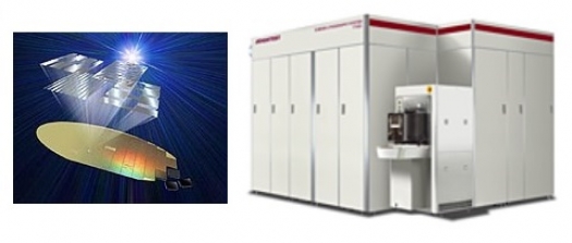
Advantest Corporation has logged its first three orders for its new EB (electron beam) lithography system, the F7000.
The company won orders from the University of Tokyo, the University of Kyoto, and a semiconductor industry customer. The systems will be shipped within the fiscal year ending March 2014.
The F7000 Series utilises electron beams to write fine-pitch patterns directly onto substrates. It offers best in class levels of throughput at the 1Xnm node, where semiconductor R&D demand is now focused.
The system's self-cleaning function ensures stable performance over long periods, while the adjuster function enables support for substrates of diverse sizes, shapes, and materials.
The customers who have ordered the F7000 Series at this time plan to use the system for R&D in the fields of MEMS/NEMS (non-electro-mechanical systems), biochips, new devices, and electronic components, in addition to research into semiconductor wafers and other forms and types of substrate.

The orders mark a milestone in Advantest's strategic expansion into new markets where its cutting-edge EB microfabrication technologies can contribute to further advances in next-generation device research and development.


