
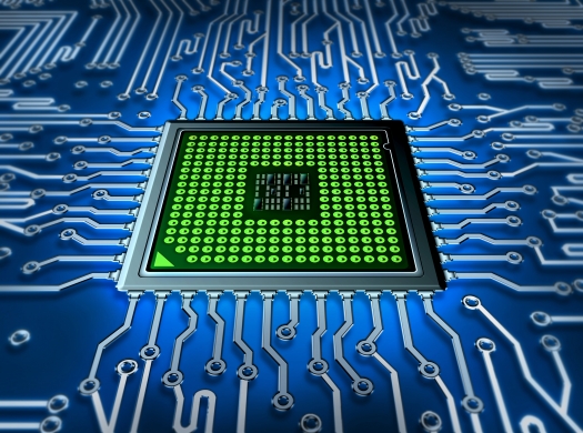
3D IC and TSV interconnect market to boom to $6.55B
Memories are anticipated to be the most promising product market with a market share of approximately 40 percent. This will be followed by sensors, in particular those used for imaging
According to a new market research report, "3D IC/Chip Market and TSV Interconnect Market," the total 3D IC market is expected to reach $6.55 billion by 2016 at a CAGR of 16.9 percent from 2011 to 2016.
The report categorises on the basis of manufacturing approaches, use of these ICs in different end-products, applications and geographical analysis; forecasting revenue and analysing trends and is published by marketsandmarkets.com.
The transition from 2D packaging to 3D packaging is considered to be one of the major developments in the semiconductor industry. 3D packaging is observed to pave the way for the concept of "More than Moore" with comparatively lesser investment.
This has led to strategic innovation with respect to 3D integration despite the economic downturn. The use of TSV interconnects within die stack instead of wirebond interconnect and board-level routing helps to save the system energy consumption to a large extent. Some of the early innovations related to TSV include those from Samsung (South Korea) and Xilinx (U.S.).
The two categories of substrates used in the production of 3D ICs include silicon on insulator (SOI) and bulk silicon. High cost is observed to be the key factor hindering the adoption of SOI wafer on a large scale. The different bonding techniques employed include die to die, die to wafer, wafer to wafer, direct bonding, adhesive bonding, and metallic bonding.
The yield achieved in wafer to wafer process is generally below 85 percent due to Known Good Die (KGD) issues and is thus observed to be cost prohibitive. In direct bonding, the wafers can be bonded at room temperature. This, in turn, helps to eliminate the problem of misalignment, which arises due to thermal expansion of one wafer relative to the other at the time of bond reaction.
With respect to process realisation techniques, it is believed that wafer to wafer and via middle processes will become the preferred standard for volume production of 3D ICs mainly due to the reduced cost of the end-product. On the other hand, via last approach can be performed with the currently available infrastructure and hence they are expected to open the path to better market adoption for 3D integration.
Amongst the various end-products for 3D ICs and TSV interconnects, the memory product market is said to have the most potential with a market share of approximately 40 percent. This is followed by sensors and in particular, image sensors. Consumer electronics application sector is observed to hold the largest share in 3D ICs and TSV interconnects market with high demand for it in a number of end-products such as smartphones, tablet PCs, e-readers, laptops, and more.
The global 3D IC market is expected to grow from $2.21 billion in 2009 to $6.55 billion in 2016 at a CAGR of 16.9 percent from 2011 to 2016 The Asian region is said to have the highest growth rate. This is mainly attributed to the presence of a huge number of companies such as TSMC (Taiwan), Samsung (South Korea), UMC (Taiwan), and more who contribute to different aspects of 3D IC manufacturing and thus help to address the challenges associated with its manufacture in a cost effective manner.


