
Nanoplas bags 14nm order and JDA with CEA-Leti
The high-selectivity dry-etch for 14nm OEM pilot line will replace wet etch. CEA-Leti will also qualify the system for additional applications
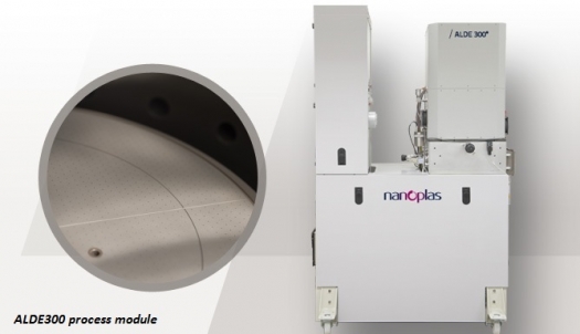
Nanoplas, a global supplier of plasma processing equipment to the semiconductor industry, has secured a second purchase order for a patented ALDE (Atomic Layer Downstream Etching) process module for extreme selectivity dielectric dry-etching.
Dielectric film removal is the process of removing an ultra-thin layer of dielectric material from a wafer's surface during the manufacturing of integrated circuits.
The company's ALDE proprietary technology provides virtually unlimited etch-rate selectivity for sub-20nm node applications in CMOS fabrication. It offers high-efficiency, lower-cost, green alternatives for treating silicon wafer surfaces in next-generation IC devices.
As the company foresees many different applications at 14nm and beyond, Nanoplas also announced a Joint Development Agreement (JDA) with CEA-Leti, extending the technology to additional applications in 14nm dry-etching, stripping and cleaning.
The new ALDE order will enable the replacement of H3PO4 wet etch with extremely selective isotropic Si3N4 dry etch in a 14nm pilot line. This first beta site in Asia will also enable significant cost-of-ownership reductions.
"We are very encouraged by this sale, in which Nanoplas offers an OEM customer a unique dry process solution to replace wet processing," explains the company's CEO, Gilles Baujon. "At the 14nm node, Nanoplas expects a massive shift from wet to dry. The drivers will be costs (chemicals, high purity water consumption and infrastructure), process performance and safety. By addressing all these challenges and targeting a range of applications, we expect ALDE to play a significant role in this shift."
To ensure that the ALDE system for extreme selectivity etching and cleaning is fully characterised and qualified in 14nm manufacturing processes, Nanoplas has signed a JDA with CEA-Leti. As part of this JDA, an ALDE tool delivery to the CEA-Leti Silicon Technology Division is scheduled for Q2 2014.
"The ALDE system offers unique performance in etching the many critical silicon-nitride spacer films in advanced transistor-formation technologies," notes CEA-Leti CEO Laurent Malier. "In this decisive final phase of development for the 14nm node, the CEA-Leti Plasma Etching & Stripping Laboratory will join forces with Nanoplas to ensure full qualification of their tool. Our experts will also help to expand the range of applications in which the ALDE technology can be used, including etching, stripping and cleaning at the 14nm node and well beyond."
Nanoplas' plasma-processing tools are used by leading microelectronics companies in North America, Europe and Asia.


