+44 (0)24 7671 8970
More publications     •     Advertise with us     •     Contact us
 
News Article

Iris AO uses MEMS technology for exceptional deformable mirrors

News

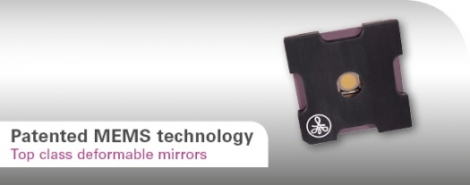
Iris AO has developed patented MEMS technology to manufacture deformable mirrors. These mirrors range from 100 to 500 actuators with inscribed aperture from 3.5 mm to 7.7 mm.

They consist of up to 163 high-quality single-crystal silicon segments. Each segment can be positioned by three actuators. Because the quality of the individual segments is so good, the gaps between the segments are small. What's more, the calibrations are so accurate, researchers have been able to show that the Iris AO deformable mirror (D) performs on par with other continuous mirrors but with huge advantages regarding the surface deformation.

A further key advantage is the wide range of optical HR coatings that can be combined with the segments. This opens DMs up to a large number of applications. Initial testing has shown that the deformable mirrors are capable of 300 W/cm2 average power handling without heat sinking and 3 kW/cm2 with heat sinking. Other tests have demonstrated peak power handling in excess of 130 MW/cm2 (4 mJ/pulse) for pulsed applications

Advantages at a glance:

    111 or 489 actuator deformable mirrors with independently controlled high-quality single-crystal silicon segments

    Factory calibrated mirror positioning "“ use it out of the box

    Optional dielectric coating for fs and high-power lasers

    Up to 10 kHz update rates

    Deliverable as complete AO system including a matched Shack-Hartmann sensor

The applications for deformable mirrors are growing steadily. Laser 2000 and Iris AO are actively developing DMs to meet the needs of new applications.

Purdue, imec, Indiana announce partnership
Resilinc partners with SEMI on supply chain resilience
NIO and NXP collaborate on 4D imaging radar deployment
Panasonic Industry digitally transforms with Blue Yonder
Global semiconductor sales decrease 8.7%
MIT engineers “grow” atomically thin transistors on top of computer chips
Keysight joins TSMC Open Innovation Platform 3DFabric Alliance
Leti Innovation Days to explore microelectronics’ transformational role
Quantum expansion
indie launches 'breakthrough' 120 GHz radar transceiver
Wafer fab equipment - facing uncertain times?
Renesas expands focus on India
Neuralink selects Takano Wafer Particle Measurement System
Micron reveals committee members
Avoiding unscheduled downtime in with Preventive Vacuum Service
NFC chip market size to surpass US$ 7.6 billion
Fujifilm breaks ground on new €30 million European expansion
Fraunhofer IIS/EAS selects Achronix embedded FPGAs
Siemens announces certifications for TSMC’s latest processes
EU Chips Act triggers further €7.4bn investment
ASE recognised for excellence by Texas Instruments
Atomera signs license agreement with STMicroelectronics
Gartner forecasts worldwide semiconductor revenue to decline 11% in 2023
CHIPS for America outlines vision for the National Semiconductor Technology Center
TSMC showcases new technology developments
Alphawave Semi showcases 3nm connectivity solutions
Greene Tweed to open new facility in Korea
Infineon enables next-generation automotive E/E architectures
Global AFM market to reach $861.5 million
Cepton expands proprietary chipset
Semtech adds two industry veterans to board of directors
Specialty gas expansion
×
Search the news archive

To close this popup you can press escape or click the close icon.
Logo
×
Logo
×
Register - Step 1

You may choose to subscribe to the Silicon Semiconductor Magazine, the Silicon Semiconductor Newsletter, or both. You may also request additional information if required, before submitting your application.


Please subscribe me to:


You chose the industry type of "Other"

Please enter the industry that you work in: