Nanoantennas increase integration in computer chips

Nanostructured metamaterials enable the reduction of the wavelength of light, allowing the creation of new types of nanophotonic devices which could advance electronics
Researchers have created tiny holograms using a "metasurface" capable of the ultra-efficient control of light, representing a potential new technology for information processing, advanced sensors and high-resolution displays.
The metasurface, thousands of V-shaped nanoantennas formed into an ultrathin gold foil, could make possible "planar photonics" devices and optical switches small enough to be integrated into computer chips for information processing, sensing and telecommunications, says Alexander Kildishev, associate research professor of electrical and computer engineering at Purdue University.
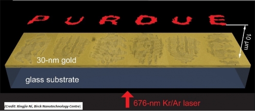
To demonstrate the technology, researchers created a hologram of the word PURDUE smaller than 100 microns wide, or roughly the width of a human hair, as shown in the picture at the top of this story.
"If we can shape characters, we can shape different types of light beams for sensing or recording, or, for example, pixels for 3D displays. Another potential application is the transmission and processing of data inside chips for information technology," Kildishev notes. "The smallest features - the strokes of the letters - displayed in our experiment are only 1 micron wide. This is a quite remarkable spatial resolution."
Metasurfaces could make it possible to use single photons - the particles that make up light - for switching and routing in future computers. While using photons would dramatically speed up computers and telecommunications, conventional photonic devices cannot be miniaturised because the wavelength of light is too large to fit in tiny components needed for integrated circuits.
Nanostructured metamaterials, however, are making it possible to reduce the wavelength of light, allowing the creation of new types of nanophotonic devices, says Vladimir M. Shalaev, scientific director of nanophotonics at Purdue's Birck Nanotechnology Centre and a distinguished professor of electrical and computer engineering.
"The most important thing is that we can do this with a very thin layer, only 30 nm, and this is unprecedented," Shalaev says. "This means you can start to embed it in electronics, to marry it with electronics."
The layer is about 1/23rd the width of the wavelength of light used to create the holograms.
Under development for about 15 years, metamaterials owe their unusual potential to precision design on the scale of nanometres. Optical nanophotonic circuits might harness clouds of electrons called "surface plasmons" to manipulate and control the routing of light in devices too tiny for conventional lasers.
The researchers have shown how to control the intensity and phase, or timing, of laser light as it passes through the nanoantennas. Each antenna has its own "phase delay" - how much light is slowed as it passes through the structure. Controlling the intensity and phase is essential for creating working devices and can be achieved by altering the V-shaped antennas.
Laser light shines through the nanoantennas, creating the hologram 10 microns above the metasurface. (Xingjie Ni, Birck Nanotechnology Centre)
The work is partially supported by U.S. Air Force Office of Scientific Research, Army research Office, and the National Science Foundation. Purdue has filed a provisional patent application on the concept.
This study has been described in detail in the paper, "Metasurface holograms for visible light," by Xingjie Ni et al in Nature Communications, 4, (2807). doi:10.1038/ncomms3807.


