
Yole: MEMS could drive future thin film PZT market
The most promising effect of thin film lead zirconium titanate (PZT) for future applications would certainly be its piezoelectric effect
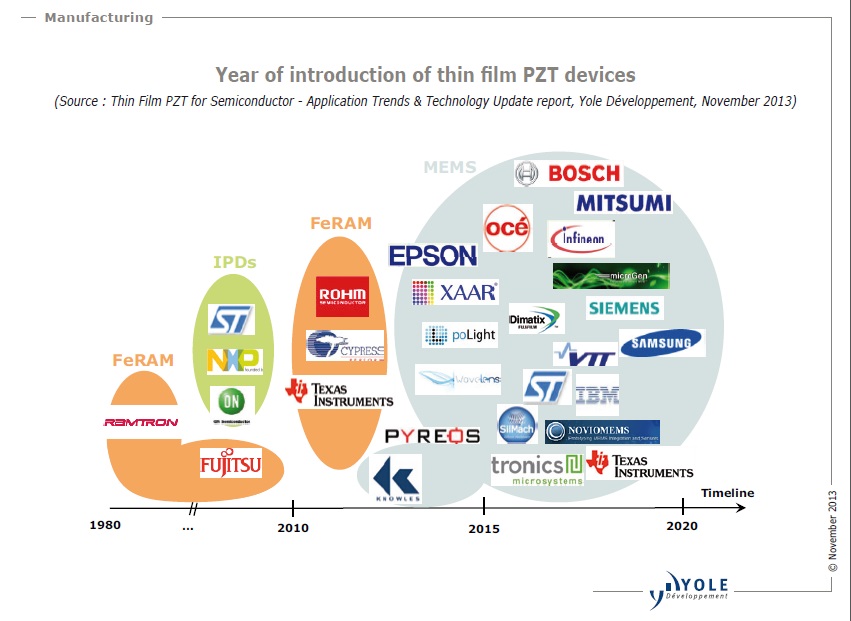
In September 2013, EPSON announced its next generation inkjet technology, PrecisionCore, introducing for the first time MEMS inkjet heads manufactured with thin film PZT technology. This announcement has been highly publicised.
First of all, thin film PZT MEMS applications are now on the market, proving the reliability and maturity of this technology. Secondly, more inkjet head players will soon follow.
This is according to the report, "Thin Film PZT for Semiconductor Application Trends & Technology Update," from Yole Développement.
"Thin film piezoelectric materials are gaining increasingly more importance within the MEMS industry. Although semiconductor manufacturing companies are historically reluctant to introduce such exotic materials into their production lines, every major MEMS foundry nowadays is working on the implementation and qualification of piezoelectric thin film in their MEMS manufacturing processes," explains Claire Troadec, Market & Technology Analyst, Semiconductor Manufacturing, at Yole Développement.
PZT, which has a chemical formula of Pb[ZrxTi1-x]O3 with 0 ≤ x ≤ 1, is a very interesting ferroelectric material. Depending on its composition, it has the advantage of combining three different material properties. It has a high dielectric constant, pyroelectric effect and piezoelectric effect.
Its high dielectric constant property is still extensively being used with the integration of thin film PZT in Integrated Passives Devices (IPDs) and to a lesser extent in Ferroelectric memories (FeRAM). These have been the two leading applications for thin film PZT for many years. NXP Semiconductors and STMicroelectronics dominate this IPD market.
The pyroelectric effect of PZT is today being used by Pyreos for thin film PZT based uncooled Infrared detectors, although this thin film PZT based technology remains quite marginal in this field.
Yole believes that the most promising effect of PZT for future applications would certainly be its piezoelectric effect.
Companies like Wavelens and PoLight are extensively working on the introduction of their autofocus based products to the market using thin film PZT technology. This profusion of new MEMS applications using thin film PZT technology is just beginning.
The roadmap for high volume production is still to be built
The main difficulty for thin film PZT technology is the integration of this exotic material into a robust and reproducible process flow. There are major technological challenges associated with thin film PZT integration into a product. These include deposition, etching, process monitoring, test and reliability.
These are complex topics and although many R&D efforts have been made so far by labs, equipment and material suppliers, and device manufacturers, some work remains to be done to achieve robust products for high volume production.
In deposition, two technologies are competing; Sol-Gel and Sputtering.
Sol-Gel gives better intrinsic film properties as deposited thin film PZT, with good uniformity and higher breakdown voltages. But when considering high volume production, throughput becomes a major consideration and this is where Sol-Gel shows some limitations.
Many equipment manufacturers within the semiconductor industry are thus working on a more classical solution; Sputtering.
ULVAC was among the first companies to develop thin film PZT deposition based on a PVD process and today, they have the more reliable PVD technology. Big semiconductor players like Applied Materials started preparing to compete in this market 18 month ago. They are rapidly ramping up their activities on thin film PZT. Meanwhile players like Oerlikon and SolMateS are continuing to improve their deposition technology, be it PVD or Pulsed Laser Deposition technology.
They both show very promising results. SolMateS is a very interesting case; with their recent PLD technology and smaller company size, they end up competing with large PVD equipment manufacturers in this thin film PZT manufacturing area.
The thin film PZT manufacturing battle is only beginning and the next five years are going to be very interesting!


