
News Article
III-V nanowires on silicon offers multiple possibilities
Due to the geometry of III-V nanowires, they could be grown directly on silicon chips in a way that alleviates restrictions due to crystal lattice mismatch - thus yielding high-quality material with the potential for high performance. If a number of hurdles are overcome, possible applications include.integrated photonics, on-chip optical interconnects amd optical transistors to speed up computers
Thread-like semiconductor structures called nanowires, so thin that they are effectively one-dimensional, show potential as lasers. These lasers could be used for applications in computing, communications, and sensing.
Now, scientists at the Technische Universität Muenchen (TUM) have demonstrated laser action in semiconductor nanowires that emit light at technologically useful wavelengths and operate at room temperature.
They have documented this breakthrough in the journal Nature Communications and in two Nano Letters papers, where they have disclosed further results showing enhanced optical and electronic performance.
"Nanowire lasers could represent the next step in the development of smaller, faster, more energy-efficient sources of light," says Jonathan Finley, director of TUM's Walter Schottky Institute.
Potential applications include on-chip optical interconnects or even optical transistors to speed up computers, integrated optoelectronics for fibre-optic communications, and laser arrays with steerable beams.
"But nanowires are also a bit special," Finley adds, "in that they are very sensitive to their surroundings, have a large surface-to-volume ratio, and are small enough, for example, to poke into a biological cell." Thus nanowire lasers could also prove useful in environmental and biological sensing.
These experimental nanowire lasers emit light in the near-infrared, approaching the "sweet spot" for fibre-optic communications. The researchers say they can be grown directly on silicon, presenting opportunities for integrated photonics and optoelectronics. And they operate at room temperature, a prerequisite for real-world applications.
Tailored in the lab, with an eye toward industry
Tiny as they are - a hundred to a thousand times thinner than a human hair - the nanowire lasers demonstrated at TUM have a complex "core-shell" cross-section with a profile of differing semiconductor materials tailored virtually atom by atom.
The nanowires' tailored core-shell structure enables them to act both as lasers, generating coherent pulses of light, and as waveguides, similar to optical fibres. Like conventional communication lasers, these nanowires are made of III-V compounds, in this case gallium arsenide- aluminium gallium arsenide (GaAs-AlGaAs) semiconductors, which have the right bandgap to emit light in the near-infrared.
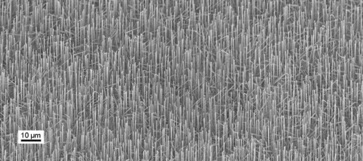
A scanning electron micrograph of the as-grown core-shell GaAs-AlGaAs nanowires revealing typical lengths ranging from 11 to 16"‰Î¼m and an areal density of the order of ~108"‰cm−2 is shown at the top of this article.
A unique advantage, Finley explains, is that the nanowire geometry is "more forgiving than bulk crystals or films, allowing you to combine materials that you normally can't combine."
Because the nanowires arise from a base only tens to hundreds of nanometres in diameter, they can be grown directly on silicon chips in a way that alleviates restrictions due to crystal lattice mismatch - thus yielding high-quality material with the potential for high performance.
Put these characteristics together, and it becomes possible to imagine a path from applied research to a variety of future applications. A number of significant challenges remain, however. For example, laser emission from the TUM nanowires was stimulated by light - as were the nanowire lasers reported almost simultaneously by a team at the Australian National University - yet practical applications are likely to require electrically injected devices.
Nanowire lasers: a technological frontier with bright prospects
The newly published results are largely due to a team of scientists who are beginning their careers, under the guidance of Gregor Koblmueller and other senior researchers, at the frontier of a new field. Doctoral candidates including Benedikt Mayer, Daniel Rudolph, Stefanie Morkötter and Julian Treu combined their efforts, working together on photonic design, material growth, and characterisation using electron microscopy with atomic resolution.

Nanowire laser researchers in the laboratory: (l-r) Benedikt Mayer, Daniel Rudolph, Gregor Koblmueller, Jonathan Finley and Gerhard Abstreiter. (Photo: A. Heddergott/TUM)
Ongoing research is directed toward better understanding the physical phenomena at work in such devices as well as toward creating electrically injected nanowire lasers, optimising their performance, and integrating them with platforms for silicon photonics.
"At present very few labs in the world have the capability to grow nanowire materials and devices with the precision required," says co-author Gerhard Abstreiter, founder of the Walter Schottky Institute and director of the TUM Institute for Advanced Study.
"And yet," he explains, "our processes and designs are compatible with industrial production methods for computing and communications. Experience shows that today's hero experiment can become tomorrow's commercial technology, and often does."
The papers in which this work has been described in detail are:
1) "Lasing from individual GaAs-AlGaAs core-shell nanowires up to room temperature," by B. Mayer et al, Nature Communications, 5th Dec. 2013. DOI: 10.1038/ncomms3931
2) "High mobility one- and two-dimensional electron systems in nanowire-based quantum heterostructures." by S. Funk et al, Nano Letters, 25th Nov. 2013. DOI: dx.doi.org/10.1021/nl403561w
3) "Enhanced luminescence properties of InAs-InAsP core-shell nanowires," by J. Treu et al, Nano Letters, 25th Nov. 2013. DOI: dx.doi.org/10.1021/nl403341x
This research was supported in part by the German Excellence Initiative through the TUM Institute for Advanced Study and the Excellence Cluster Nanosystems Initiative Munich (NIM); by the German Research Foundation (DFG) through Collaborative Research Centre SFB 631; by the European Union through a Marie Curie European Reintegration Grant, the QUROPE project SOLID, and the EU-MC network INDEX; by a CINECA award under the ISCRA initiative; and by a grant from Generalitat Valenciana.
Now, scientists at the Technische Universität Muenchen (TUM) have demonstrated laser action in semiconductor nanowires that emit light at technologically useful wavelengths and operate at room temperature.
They have documented this breakthrough in the journal Nature Communications and in two Nano Letters papers, where they have disclosed further results showing enhanced optical and electronic performance.
"Nanowire lasers could represent the next step in the development of smaller, faster, more energy-efficient sources of light," says Jonathan Finley, director of TUM's Walter Schottky Institute.
Potential applications include on-chip optical interconnects or even optical transistors to speed up computers, integrated optoelectronics for fibre-optic communications, and laser arrays with steerable beams.
"But nanowires are also a bit special," Finley adds, "in that they are very sensitive to their surroundings, have a large surface-to-volume ratio, and are small enough, for example, to poke into a biological cell." Thus nanowire lasers could also prove useful in environmental and biological sensing.
These experimental nanowire lasers emit light in the near-infrared, approaching the "sweet spot" for fibre-optic communications. The researchers say they can be grown directly on silicon, presenting opportunities for integrated photonics and optoelectronics. And they operate at room temperature, a prerequisite for real-world applications.
Tailored in the lab, with an eye toward industry
Tiny as they are - a hundred to a thousand times thinner than a human hair - the nanowire lasers demonstrated at TUM have a complex "core-shell" cross-section with a profile of differing semiconductor materials tailored virtually atom by atom.
The nanowires' tailored core-shell structure enables them to act both as lasers, generating coherent pulses of light, and as waveguides, similar to optical fibres. Like conventional communication lasers, these nanowires are made of III-V compounds, in this case gallium arsenide- aluminium gallium arsenide (GaAs-AlGaAs) semiconductors, which have the right bandgap to emit light in the near-infrared.
A scanning electron micrograph of the as-grown core-shell GaAs-AlGaAs nanowires revealing typical lengths ranging from 11 to 16"‰Î¼m and an areal density of the order of ~108"‰cm−2 is shown at the top of this article.
A unique advantage, Finley explains, is that the nanowire geometry is "more forgiving than bulk crystals or films, allowing you to combine materials that you normally can't combine."
Because the nanowires arise from a base only tens to hundreds of nanometres in diameter, they can be grown directly on silicon chips in a way that alleviates restrictions due to crystal lattice mismatch - thus yielding high-quality material with the potential for high performance.
Put these characteristics together, and it becomes possible to imagine a path from applied research to a variety of future applications. A number of significant challenges remain, however. For example, laser emission from the TUM nanowires was stimulated by light - as were the nanowire lasers reported almost simultaneously by a team at the Australian National University - yet practical applications are likely to require electrically injected devices.
Nanowire lasers: a technological frontier with bright prospects
The newly published results are largely due to a team of scientists who are beginning their careers, under the guidance of Gregor Koblmueller and other senior researchers, at the frontier of a new field. Doctoral candidates including Benedikt Mayer, Daniel Rudolph, Stefanie Morkötter and Julian Treu combined their efforts, working together on photonic design, material growth, and characterisation using electron microscopy with atomic resolution.
Nanowire laser researchers in the laboratory: (l-r) Benedikt Mayer, Daniel Rudolph, Gregor Koblmueller, Jonathan Finley and Gerhard Abstreiter. (Photo: A. Heddergott/TUM)
Ongoing research is directed toward better understanding the physical phenomena at work in such devices as well as toward creating electrically injected nanowire lasers, optimising their performance, and integrating them with platforms for silicon photonics.
"At present very few labs in the world have the capability to grow nanowire materials and devices with the precision required," says co-author Gerhard Abstreiter, founder of the Walter Schottky Institute and director of the TUM Institute for Advanced Study.
"And yet," he explains, "our processes and designs are compatible with industrial production methods for computing and communications. Experience shows that today's hero experiment can become tomorrow's commercial technology, and often does."
The papers in which this work has been described in detail are:
1) "Lasing from individual GaAs-AlGaAs core-shell nanowires up to room temperature," by B. Mayer et al, Nature Communications, 5th Dec. 2013. DOI: 10.1038/ncomms3931
2) "High mobility one- and two-dimensional electron systems in nanowire-based quantum heterostructures." by S. Funk et al, Nano Letters, 25th Nov. 2013. DOI: dx.doi.org/10.1021/nl403561w
3) "Enhanced luminescence properties of InAs-InAsP core-shell nanowires," by J. Treu et al, Nano Letters, 25th Nov. 2013. DOI: dx.doi.org/10.1021/nl403341x
This research was supported in part by the German Excellence Initiative through the TUM Institute for Advanced Study and the Excellence Cluster Nanosystems Initiative Munich (NIM); by the German Research Foundation (DFG) through Collaborative Research Centre SFB 631; by the European Union through a Marie Curie European Reintegration Grant, the QUROPE project SOLID, and the EU-MC network INDEX; by a CINECA award under the ISCRA initiative; and by a grant from Generalitat Valenciana.


