
Shrink fifty metres of optical fibre to microchip size
DARPA's iPhoD program has concluded with a demonstration of low signal loss records with microchip-scale, integrated waveguides for photonic delay
Long coils of optical waveguides - any structure that can guide light, like conventional optical fibre - can be used to create a time delay in the transmission of light.
Such photonic delays are useful in military applications ranging from small navigation sensors to wideband phased array radar and communication antennas.
Although optical fibre has extremely low signal loss, an advantage that enables the backbone of the global Internet, it is limited in certain photonic delay applications.
Connecting fibre optics with microchip-scale photonic systems requires sensitive, labour-intensive assembly and a system with a large number of connections suffers from signal loss.
Recently, DARPA-funded researchers have developed new methods to integrate long coils of waveguides with low signal loss onto microchips - potentially enabling a leap ahead in size reduction and performance.
DARPA's integrated Photonic Delay (iPhoD) program created a new class of photonic waveguides with losses approaching that of optical fibre. The new waveguides are built onto microchips and include up to 50 metres of coiled material that is used to delay light.
Conventional fibre optic coils of the same length would be about the size of a small juice glass. But these waveguides, which also employ modern silicon processing to achieve submicron precision and more efficient manufacturing, result in a new component that is smaller and more precise than anything before in its class.
"Prior to the start of iPhoD, the best integrated waveguides had a signal loss of about 1 decibel per metre with total lengths of only a few metres," notes Josh Conway, DARPA program manager. "Under iPhoD, two research teams created chips with loss around 0.05 decibels per metre. The sub-millimetre bend diameter, which describes how tightly the waveguide can coil without significant signal loss, allowed the demonstration of a 50-metre optical delay on a single microchip."
The iPhoD project concluded recently with successful demonstrations by research teams led by the University of California, Santa Barbara (UCSB) and the California Institute of Technology (CalTech).
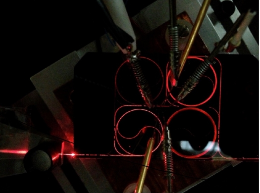
The ultra-low loss, true-time delay chip developed at UCSB is composed of silicon nitride (SiN). The chip, which has four different delay lines. is pictured at the top of this story.
Selecting this material may allow for integration with a variety of devices and materials - thereby reducing size, weight and power requirements of an overall system. UCSB researchers also demonstrated 3D waveguide stacking, enabling more waveguide length, and thus, longer photonic delays.
Researchers at CalTech had a different approach for a chip-scale waveguide, as reported in the Nature Communications paper, "Ultra-low-loss optical delay line on a silicon chip." The CalTech waveguide was constructed from silicon oxide, commonly known as glass, and demonstrated low loss over twenty seven metres.

Scanning electron micrograph of iPhod waveguide from the California Institute of Technology
"These results are firsts for optical waveguides with performance that is equal or superior to larger, fibre optic-based devices," concludes Conway. "Chip-scale waveguides, with smaller sizes and new integration possibilities promise advanced, compact military systems such as tactical gyroscopes that significantly outperform state-of-the-art MEMS devices with the same footprint."


