
Nanoscale discovery has major implications for chip manufacturers
The main processes used to transform properties of nanoscale materials could cause much greater damage than previously believed
Manufacturers of increasingly minute computer chips, transistors and other semiconductor products may find research findings at the University of Huddersfield useful.
The implications are that a key process used to transform the properties of nanoscale materials can cause much greater damage than previously realised.
The University is home to the Electron Microscopy and Materials Analysis Research Group (EMMA), headed by Stephen Donnelly. It has an advanced facility named MIAMI (Microscope and Ion Accelerators for Materials Investigation). MIAMI is used to bombard materials with ion beams and to examine the effects at the nanoscale.
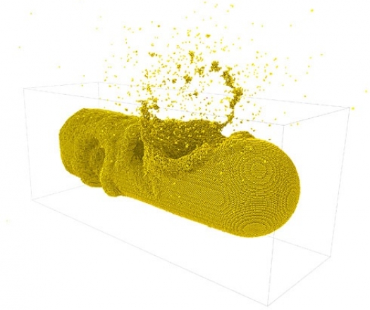
During a recent experiment conducted by the team, including Research Fellow Graeme Greaves, a number of gold nanorods - a thousand times smaller than a human hair - were irradiated with xenon atoms. They were a good subject for the experiment because nanowires or rods have a large surface area.

Graeme Greaves, University of Huddersfield
The findings were dramatic.
"We were hoping to generate bubbles. We actually found that we were eroding the nanowires," says Greaves.
Kai Nordlund of the University of Helsinki who verified the research of the University of Huddersfield's Graeme Greaves into gold nanoparticles sputtering yield. And the rate of erosion - measured in terms of 'sputtering yield', or how many atoms come out of matter for each incoming atom - was far in advance of expectations.
"The sputtering yield of a normal piece of flat gold should be of the order of fifty atoms per ion," says Greaves. "In the case of rods we expected it to be greater, because the geometry is much reduced. We worked out that it should be higher by a factor of four, or something of that order. But we actually found that the greatest value measured was a sputtering yield of a thousand - a factor of twenty."
The results were so dramatic that the Huddersfield team sought confirmation. They asked Kai Nordlund of the University of Helsinki to run a molecular dynamics simulation, creating a virtual gold nanorod. The Finns were able to replicate the Huddersfield findings.

Kai Nordlund, University of Helsinki
Now the experiment is the subject of an article in the journal Physical Letters Review.
"The research has considerable implications, particularly for medicine," says Greaves. "More and more people are working on nanostructures for practical applications. Gold nanoparticles can be used for tumour detection, the optimisation of the bio-distribution of drugs to diseased organs and a radiotherapy dose enhancer.
He adds, "Components of computer chips are very small nowadays - in the order of 20 nanometres in size and getting smaller - and ion beams are used to change the properties of these materials. Our research shows you must be very wary of the amount of damage that may be done."
This work has been described in depth in the paper, "Enhanced Sputtering Yields from Single-Ion Impacts on Gold Nanorods," by G. Greaves et al in Physical Review Letters 111, 065504 (2013).
DOI: 10.1103/PhysRevLett.111.065504


