
Organic transistor rivals silicon in see-through electronics
Researchers in the U.S. have collaborated to make thin, transparent semiconductors that could become the foundation for cheap, high-performance displays
Two university research teams have worked together to produce what they claim are the world's fastest thin-film organic transistors.
They believe this proves that this experimental technology has the potential to achieve the performance needed for high-resolution television screens and similar electronic devices.
For years engineers the world over have been trying to use inexpensive, carbon-rich molecules and plastics to create organic semiconductors capable of performing electronic operations at something approaching the speed of costlier technologies based on silicon.
The term "organic" was originally confined to compounds produced by living organisms but now extended to include synthetic substances based on carbons and includes plastics.
In the January 8th edition of Nature Communications, engineers from the University of Nebraska-Lincoln (UNL) and Stanford University show how they created thin-film organic transistors that could operate more than five times faster than previous examples of this experimental technology.
Research teams led by Zhenan Bao, professor of chemical engineering at Stanford, and Jinsong Huang, assistant professor of mechanical and materials engineering at UNL used their new process to make organic thin-film transistors with electronic characteristics comparable to those found in expensive, curved-screen television displays based on a form of silicon technology.

Professor Zhenan Bao led a team that has developed the world's fastest organic thin-film transistors. (Joel Simon)
They achieved their speed boost by altering the basic process for making thin-film organic transistors.
Typically, researchers drop a special solution, containing carbon-rich molecules and a complementary plastic, onto a spinning platter "“ in this case, one made of glass. The spinning action deposits a thin coating of the materials over the platter.
In their Nature Communications paper, the collaborators describe two important changes to this basic process.
First they spun the platter faster. Second they only coated a tiny portion of the spinning surface, equivalent to the size of a postage stamp.
These innovations had the effect of depositing a denser concentration of the organic molecules into a more regular alignment. The result was a great improvement in carrier mobility, which measures how quickly electrical charges travel through the transistor.
The researchers called this improved method "off-centre spin coating." The process remains experimental, and the engineers cannot yet precisely control the alignment of organic materials in their transistors or achieve uniform carrier mobility.
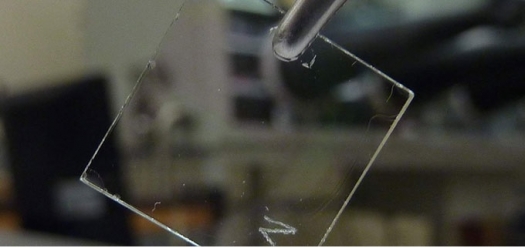
The picture at the top of this story shows transparent transistors on a postage-stamp size glass which have speed characteristics rivalling some forms of silicon transistors. The device used a new process to make this world record-setting organic transistor, paving the way for a new generation of cheap, transparent electronic devices. (Image courtesy of Jinsong Huang and Yongbo Yuan).
Even at this stage, off-centre spin coating produced transistors with a range of speeds much faster than those of previous organic semiconductors and comparable to the performance of the polysilicon materials used in today's high-end electronics.
Further improvements to this experimental process could lead to the development of inexpensive, high-performance electronics built on transparent substrates such as glass and, eventually, clear and flexible plastics.
Already, the researchers have shown that they can create high-performance organic electronics that are ninety percent transparent to the naked eye.
The study is described in detail in the paper, "Ultra-high mobility transparent organic thin film transistors grown by an off-centre spin-coating method," by Yongbo Yuan et al in Nature Communications, 5, 3005 , published on 8th January 2014. doi:10.1038/ncomms4005
This work was funded by the U.S. Defence Advanced Research Projects Agency (DARPA), the Air Force Office of Scientific Research and the National Science Foundation.


