+44 (0)24 7671 8970
More publications     •     Advertise with us     •     Contact us
 
News Article

Towa opens new packaging development centre

News
The facility will cater for packaging a number of products including MEMS for European customers


The Towa Corporation of Japan has established its activities in Europe with an Innovation Centre for Packaging Development.

Towa is a supplier of packaging equipment for the semiconductor, electronics and LED industries.

Europe has become an area where special IC´s and electronic applications are being developed and produced, such as sensors, MEMS, vision applications, specific IC’s, in particular for semiconductor, automotive and medical applications.

In 2004 Towa Europe GmbH was established, to serve European customers. The activities originally consisted of the supply of the Towa encapsulation equipment, after sales service and spare parts.

However, in addition to this, the cooperation with the package/product development centres of European customers and European institutes became an important activity and Towa Europe started to play a leading role in the development of new products.

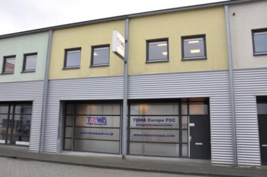
To further expand this, it was decided to establish a Packaging Development Centre in the Netherlands, for which Towa Europe has been founded. This centre is located at Geograaf 14, Duiven, The Netherlands.


Towa Laboratory

A fully equipped laboratory with two Towa molding systems, test and measuring equipment as well as an engineering department is available to give full support in all the phases of product development, from initial concept up to test, qualification and industrialisation.

The Dutch, German and English speaking staff will be happy to assist European customers with the exciting process of new package development. Also the European Marketing, Sales and Service department for the Towa systems is located at this new facility.

 
Purdue, imec, Indiana announce partnership
Resilinc partners with SEMI on supply chain resilience
NIO and NXP collaborate on 4D imaging radar deployment
Panasonic Industry digitally transforms with Blue Yonder
Global semiconductor sales decrease 8.7%
MIT engineers “grow” atomically thin transistors on top of computer chips
Keysight joins TSMC Open Innovation Platform 3DFabric Alliance
Leti Innovation Days to explore microelectronics’ transformational role
Quantum expansion
indie launches 'breakthrough' 120 GHz radar transceiver
Wafer fab equipment - facing uncertain times?
Renesas expands focus on India
Neuralink selects Takano Wafer Particle Measurement System
Micron reveals committee members
Avoiding unscheduled downtime in with Preventive Vacuum Service
NFC chip market size to surpass US$ 7.6 billion
Fujifilm breaks ground on new €30 million European expansion
Fraunhofer IIS/EAS selects Achronix embedded FPGAs
Siemens announces certifications for TSMC’s latest processes
EU Chips Act triggers further €7.4bn investment
ASE recognised for excellence by Texas Instruments
Atomera signs license agreement with STMicroelectronics
Gartner forecasts worldwide semiconductor revenue to decline 11% in 2023
CHIPS for America outlines vision for the National Semiconductor Technology Center
TSMC showcases new technology developments
Alphawave Semi showcases 3nm connectivity solutions
Greene Tweed to open new facility in Korea
Infineon enables next-generation automotive E/E architectures
Global AFM market to reach $861.5 million
Cepton expands proprietary chipset
Semtech adds two industry veterans to board of directors
Specialty gas expansion
×
Search the news archive

To close this popup you can press escape or click the close icon.
Logo
×
Logo
×
Register - Step 1

You may choose to subscribe to the Silicon Semiconductor Magazine, the Silicon Semiconductor Newsletter, or both. You may also request additional information if required, before submitting your application.


Please subscribe me to:


You chose the industry type of "Other"

Please enter the industry that you work in: