Improving microscopy on the atomic scale

Now microscopy researchers at North Carolina State University have developed a new technique that accounts for that movement and eliminates the distortion from the finished product.
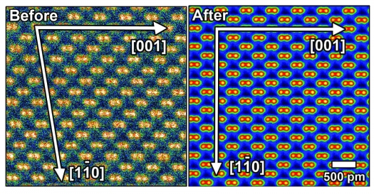
The new technique effectively eliminates distortion from nanoscale images as shown in the image at the top of this article.
At issue are scanning transmission electron microscopes (TEMs), which can capture images of a material's individual atoms. To take those images, scientists have to allow a probe to scan across the sample area - which has an area of less than twenty five nanometres squared. That scanning can take tens of seconds.
TEM is very useful for observing dislocations and measuring layer thicknesses in semiconductors.
The sample rests on a support rod, and while the scanning takes place the rod expands or contracts due to subtle changes in ambient temperature. The rod's expansion or contraction is imperceptible to the naked eye, but because the sample area is measured in nanometres the rod's movement causes the sample material to shift slightly. This so-called "drift" can cause the resulting scanning TEM images to be significantly distorted.
"But our approach effectively eliminates the effect of drift on scanning TEM images," says James LeBeau, an assistant professor of materials science and engineering at NC State and senior author of a paper describing the work.
Researchers programmed the microscope to rotate the direction in which it scans the sample. For example, it might first take an image scanning from left to right, then take one scanning from top to bottom, then right to left, then bottom to top. Each scanning direction captures the distortion caused by drift from a different vantage point.
The researchers plug those images into a program they developed that measures the features in each image and uses that data to determine the precise direction and extent of drift within the sample. Once the drift is quantified, the images can be adjusted to remove the distortion caused by the drift.
The resulting images accurately represent the actual structure of the sample and give scientists new capabilities to understand bonding between atoms.
"Historically, a major problem with drift has been that you need to have a reference material in any nanoscale image, so that you can tell how the image has been distorted," LeBeau says. "This technique makes that unnecessary. That means we can now look at completely unknown samples and discover their crystalline structures - which is an important step in helping us control a material's physical properties."
The paper, "Revolving scanning transmission electron microscopy: correcting sample drift distortion without prior knowledge," by Xiahan Sang et al will be published in the March issue of Ultramicroscopy.
There is a patent pending on the technique.


