
Graphene challenges silicon for mobile devices
Graphene's unique properties make it suited for wireless or radio frequency communications. It's properties could make it less expensive and more energy efficient than silicon
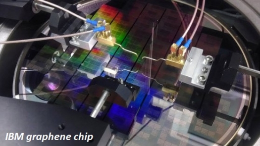
An IBM lab in New York has built a rudimentary semiconductor chip with circuits made from graphene, a crystalline version of carbon that takes on a honeycomb lattice shape on an atomic scale. And if successful, this could have significant implications for mobile devices.

IBM graphene chip
The advance is the latest application of nanotechnology, or physical materials that are as small at a billionth of a metre, in semiconductor chips that are the foundation of everything electronic.
Nanotechnology solutions such as graphene are like designer molecules that could make chips smaller, faster, and much more power efficient than today's silicon chips. But the technology is still in its experimental stage because scientists still have a tough time getting nanotech materials to behave properly on an atomic scale.
The team at IBM Research in Yorktown Heights, N.Y., has built the most advanced, fully functional graphene integrated circuit with possible applications in wireless communications. If they work properly, graphene-based chips could enable mobile devices such as smartphones, tablets, or wearable electronics to transmit much faster data loads to each other and to their surroundings.
They could also do so in a more cost-effective and power-efficient manner compared to traditional technology solutions. The team has used the graphene circuit to send a text message with the letters "I-B-M" as you would with a smartphone. That just shows it works in a wireless communications application.

Graphene molecules with chip circuits
IBM says the nanotechnology milestone opens up new carbon-based electronics device and circuit applications beyond what is possible with today's silicon chips. Graphene's unique properties make it suited for wireless or radio frequency communications. It has admirable electrical, optical, mechanical, and thermal properties that could make it less expensive and more energy efficient than silicon, which has been in use for more than fifty years.
IBM says graphene radio devices could enable pervasive wireless communications, such as cheap smart sensors and radio frequency identification tags that send signals over long distances. Right now, RFID tags have extremely limited range.
Graphene is easily damaged in manufacturing, so making an integrated circuit from it is hard. But IBM first demoed a prototype in 2011 and have now improved it.
Using mainstream silicon manufacturing techniques, a team of IBM researchers have solved one big problem and tested the world's first multistage graphene radio-frequency receiver, the most sophisticated graphene integrated circuit to date. The performance is 10,000 times better than previous reported results for graphene chips.
"This is the first time that someone has shown graphene devices and circuits to perform modern wireless communication functions comparable to silicon technology," says Supratik Guha, the director of physical sciences at IBM Research. The work was funded by the Defence Advanced Research Communications Agency and was reported in a paper in the journal Nature Communications.

IBM graphene chip up close


