Extending Moore's law with III-Vs

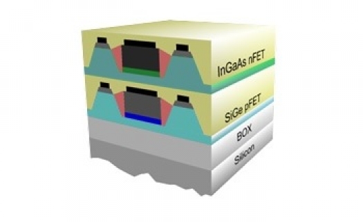
European scientists will use compound semiconductors indium gallium arsenide and silicon germanium and design concepts to demonstrate a working prototype of a new type of 3D-stacked hybrid SRAM cell
Scientists from both academia and industry have begun an ambitious new research project focused on an alternative approach to extend Moore's Law.
The goal is to reduce costs and improve the energy efficiency of electronic devices ranging from mobile phones to supercomputers. The research project, called COMPOSE³, is based on the use of new materials to replace today's silicon, and on taking an innovative design approach where transistors are stacked vertically, known as 3D stacking.
Coordinated by IBM Research in Zurich, COMPOSE3 is a scientific collaboration among industry, research organisations and small- and medium-size enterprises from six European countries: STMicroelectronics, CEA-Leti and the Centre National de la Recherche Scientifique in France; University of Glasgow in the UK; Tyndall National Institute at University College Cork in Ireland; DTF Technology GmbH in Germany; and Fundación IMDEA Materiales in Spain.
Moore's Law predicted that the number of transistors that can be placed on an integrated circuit will double every eighteen months, leading to a drastic reduction in the cost per digital function. First observed more than fifty years ago, this law has now reached its limits due to shrinking chip geometries.
For example a processor's clock speed has barely increased in the past five years, with typical operating frequencies at 2 to 3 GHz. In addition, energy consumption of electronic devices is growing at a staggering rate with estimates reporting that it accounts for up to 10 percent of the total electrical energy generated in industrialized countries.
To address these challenges, scientists will develop a static random-access memory (SRAM) cell based on two novel materials, indium gallium arsenide (InGaAs) and silicon germanium (SiGe), which replace silicon in the heart of the transistor.
SRAM is an essential circuit component found in processors in a wide range of applications from smartphones to high-performance computers, and is usually built of two different types of transistors, called nFET and pFET. In COMPOSE3, the nFET will use InGaAs, whereas the pFET will use SiGe.
An SRAM cell has therefore been selected as the ideal test vehicle to demonstrate this kind of hybrid technology. As charge carriers can move faster in InGaAs and SiGe than in silicon alone, the transistors can also be operated at a lower voltage, greatly reducing the power consumption of digital circuits.
The unique chemical properties of InGaAs and SiGe also offer the possibility to stack transistors vertically at the nanometre scale, opening new avenues to increase the number of devices per unit area, while reducing the manufacturing costs for each transistor.
"This technology will provide a new paradigm shift in density scaling combined with a dramatic increase in the power efficiency of CMOS circuits. Our synergistic approach is based on replacing silicon with high-mobility channel materials such as SiGe and InGaAs," says Jean Fompeyrine, manager of the Advanced Functional Materials group at IBM Research - Zurich.
"Using these materials in a technology that delivers performance at low power and at the same time provides a density increase at reduced costs is a fantastic challenge that requires the collective knowledge of both industry and academia," continues Fompeyrine.
Indeed, the challenges associated with this approach are significant, particularly with regard to the minimisation of electrically active defects in the vicinity of InGaAs and SiGe, the fabrication of transistors with low-resistance contact, and thermal management during 3D stacking. The consortium partners each bring specific expertise to support this major European innovation.
Within three years the team of scientists expects to unveil a proof of concept for building the world's first 14nm 3D-stacked SRAM cell based on InGaAs and SiGe materials. The project will also demonstrate that the technology can be manufactured using standard processes in the microelectronics industry.
COMPOSE3 is a €4.7 million project, with €3.2 million funded by the European Union's Seventh Framework Program (FP7). COMPOSE3 started in January of 2014 and will run for three years.


