
EVG enhances memory photoresist manufacturing
The firm's new technology system is targeted for logic and memory advanced packaging applications
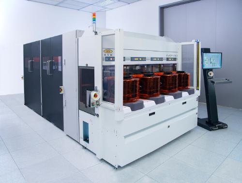
EV Group (EVG) has unveiled its most advanced 300 mm photoresist processing system for logic and memory high-volume manufacturing (HVM).
This is the EVG150XT resist coating and developing system.
Leveraging EVG's XT Frame platform utilized across the spectrum of the company's industry-leading systems, the EVG150XT is optimised for ultra-high throughput and productivity - bringing the company's expertise in lithography processing to HVM environments.
The EVG150XT is designed for processing resists, spin-on dielectrics and thick films for mid-end-of-line (MEOL) and back-end-of-line (BEOL) semiconductor applications, including through silicon via (TSV) formation, wafer bumping, redistribution layer and interposer manufacturing for 2.5 and 3D-IC packaging.
As 2.5/3D packaging moves closer to production reality in the semiconductor industry in order to integrate increasing amounts of chip functionality in smaller form factors for mobile devices and other consumer electronic products, new manufacturing and cost requirements must be addressed across the wafer fabrication process-particularly in the MEOL and BEOL segments.
Smaller pitches, copper pillars, the formation of redistribution layers to enable chip-to-chip connections utilizing under bump metallisation, and the connection of dies produced with different design-node processes, have led to tighter standards in process uniformity.
As the industry ramps to volume production on these devices, the wafer processing equipment used to manufacture these devices will require both enhanced throughput and processing capabilities.
The EVG150XT features nine process modules that can operate simultaneously for multi-parallel wafer processing. Smart scheduling software for throughput-optimized handling sequences has also been incorporated, along with pumps and dispense systems tailored for thick film applications.
In addition, an in-line metrology module has been integrated into the EVG150XT that can detect a variety of process irregularities and defects to enable real-time process corrections to reduce defects, increase yields and lower production costs. These and other software and hardware enhancements optimize the EVG150XT for high-volume manufacturing environments.
"For the past 30 years, EV Group has built up significant process know-how in both lithography and HVM processing working closely with our customers and turning their feedback into new capabilities built into our next-generation products. With our latest product introduction - the EVG150XT - we've successfully combined both areas of expertise to provide our customers with the industry's first true HVM resist processing system that can meet their most demanding requirements for mid-end and back-end-of-line applications," states Paul Lindner, executive technology director at EV Group.
Media and analysts interested in learning more about EVG's latest developments in photoresist and lithography processing, as well as other high-volume manufacturing solutions, are invited to visit the company's booth #1264 in Hall C at the COEX Convention and Exhibitor Centre in Seoul, Korea at the SEMICON Korea show on from February 12th to 14th.


