
CEA-Leti acquires Rudolph's new TSV metrology system
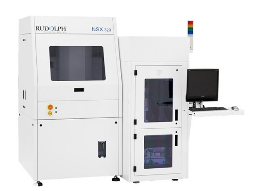
The first NSX 320 metrology system has been sold specifically for Through Silicon Via (TSV) process development. It includes specialised sensors to measure critical parameters in 3D integration
Rudolph Technologies has sold its first NSX 320 TSV Metrology System to CEA-Leti, a research organisation based in Grenoble, France.
In the frame of the Nanoelec Research Technology Institute (Nanoelec RTI) program, CEA-Leti is developing three-dimensional integrated circuit (3DIC) technologies that use TSVs to conduct signals among vertically-stacked chips.
The new NSX 320 TSV system includes integrated 3D metrology that enables specialised measurements critical to the TSV process.
"Controlling the processes used to create TSVs requires a number of specialised measurements, such as the total thickness variation (TTV) of the wafer bonded to the carrier, or the remaining silicon thickness after thinning," says Séverine Cheramy, CEA-Leti's director of 3D integration development in the Nanoelec RTI program. "The NSX system's 3D metrology capabilities, which combine accurate 2D measurements with the ability to see and measure front, back and internal interface surfaces, will provide critical information for our TSV development program."
Matt Wilson, Rudolph's NSX Series product manager adds, "Three-dimensional integration using TSVs is widely expected to be a key technology enabling our industry to maintain the incredible pace of development and innovation first described as Moore's Law nearly fifty years ago. Ultimately we see the potential for rapid growth in this segment and are pleased to be part of the pioneering efforts of a leading research organisation like CEA-Leti."
Rudolph's NSX TSV metrology systems combine the NSX family's well-established 2D inspection capabilities with an advanced 3D metrology that was developed at recently-acquired Tamar Technology.
Together, they allow the NSX metrology system to perform a wide variety of measurements needed to characterize and control TSV processes, including TSV depth measurements, bottom CD measurements, pre- and post-thinning remaining silicon thickness measurements during the reveal process, copper nail height measurements, edge trim monitoring, adhesive TTV of bonded pairs and product wafers, and traditional defect inspection throughout the entire process.


