
Gigaphoton laser to enable G450C with 450mm lithography
This marks a step in demonstrating the capability of Gigaphoton's most advanced high-power GT64A light source for high volume production in 450mm lithography processes
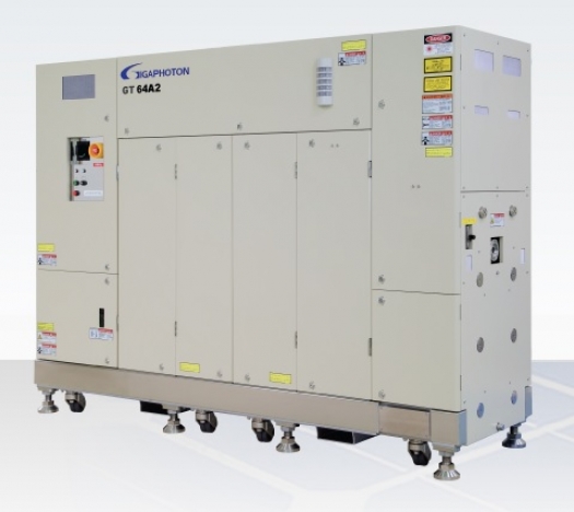
Gigaphoton's high-power ArF Immersion Laser (GT64A) will be used by the Global 450 Consortium (G450C), headquartered at SUNY's College of Nanoscale Science and Engineering (CNSE) in Albany, New York, as the light source for its first 450mm ArF Immersion lithography scanners.
The laser will be used for both off-site and on-site development and testing, as well as technology demonstrations at CNSE's G450C facility. Delivery of the laser to CNSE is expected in April 2015.
G450C is a public-private partnership announced by New York Governor Andrew M. Cuomo in September 2011 to facilitate the 450mm wafer size transition. G450C is spearheaded by CNSE in partnership with Intel, IBM, GLOBALFOUNDRIES, Samsung and TSMC. The new 450mm cleanroom is located at CNSE's Albany NanoTech Complex within the NanoFab Xtension (NFX) expansion.
The GT64A can achieve a power output of up to 120W for multi-patterning in 450mm wafer production applications. The light energy output can be automatically adjusted to optimum levels based on each customer's process.
The GT6 A incorporates a stable energy, spectral bandwidth, wavelength, and beam profile, combined with improved overlay accuracy, critical dimension control, and minimisation of line-edge roughness - all of which are extremely important for multi-patterning lithography.
The GT64A's product concept also relies heavily on eco-friendliness, minimising the consumption and cost of electricity, gas, and cooling (facilities) resources.
Paul Farrar, Jr., CNSE Vice President for Manufacturing Innovation and General Manager of G450C, says, "Under the leadership and vision of Governor Andrew Cuomo, New York is firmly established as the hub for the critical industry evolution to 450mm wafer technology. We look forward to working closely with Gigaphoton Inc., and to utilizing its technology and capabilities to help enable the important transition to 450mm technology."
"We are very excited by this opportunity to be a part of the critical and ground-breaking work led by G450C," continues enthusiastic Hitoshi Tomaru, President and CEO of Gigaphoton. "This represents yet another important achievement in Gigaphoton's long-standing commitment to offering the products, services, and technical solutions necessary to sustain a healthy, high-volume manufacturing environment and roadmap. We are committed to continuing to invest in the research and development of advanced lithography technologies, including technologies for minimising environmental impact through our EcoPhoton program."
The G450C is a public-private partnership program comprising New York State (CNSE), Intel, TSMC, Samsung, IBM and GlobalFoundries that is developing a cost-effective test wafer fabrication infrastructure, equipment prototypes and high-volume tools to enable a coordinated industry transition to 450mm wafers.


