+44 (0)24 7671 8970
More publications     •     Advertise with us     •     Contact us
 
News Article

Fujitsu expands its memory range

News

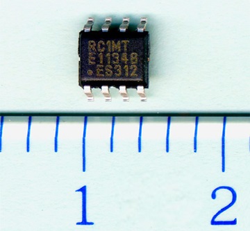
Fujitsu Semiconductor America (FSA) has introduced the latest in its family of FRAMs. The MB85RC1MT has 1 Mbit of memory.

This, FSA says, is the highest memory capacity of the company's products with an I2C serial interface.

The new MB85RC1MT is an excellent design choice for applications requiring frequent rewriting of data, such as real-time data logging for factory-automation, instrumentation, and industrial equipment. It operates between 1.8V and 3.3V in temperature ranges between -400C and 850C.

It supports 'high-speed' mode, which enables read and write at operating frequencies of 3.4MHz and at 1MHz, the same speed as conventional EEPROMs. The new FRAM guarantees ten trillion write-erase cycles, which significantly exceeds the ability of EEPROMs. It can replace EEPROMs to enable high-precision data capture and reduced power consumption during data writing.

FRAM's non-volatility means that data is retained even when the power is switched off. Random access to its memory cells enables rapid data writing.

Since Fujitsu Semiconductor began volume production of FRAM products in 1999, these features have led to the wide use of FRAMs in applications such as factory automation equipment, instrumentation, financial terminals, and medical devices.

The development of the MB85RC1MT adds to Fujitsu's FRAM products that use the I2C interface covering a full range from 4 Kbit to 1 Mbit.

In addition, FRAMs with the SPI interface range from 16 Kbit to 2 Mbits. All are offered in industry-standard 8-pin SOP packages to replace EEPROMs and serial Flash memories in a broad variety of applications with no need for major changes in PCB design.

Samples of the new MB85RC1MT are available now.


Purdue, imec, Indiana announce partnership
Resilinc partners with SEMI on supply chain resilience
NIO and NXP collaborate on 4D imaging radar deployment
Panasonic Industry digitally transforms with Blue Yonder
Global semiconductor sales decrease 8.7%
MIT engineers “grow” atomically thin transistors on top of computer chips
Keysight joins TSMC Open Innovation Platform 3DFabric Alliance
Leti Innovation Days to explore microelectronics’ transformational role
Quantum expansion
indie launches 'breakthrough' 120 GHz radar transceiver
Wafer fab equipment - facing uncertain times?
Renesas expands focus on India
Neuralink selects Takano Wafer Particle Measurement System
Micron reveals committee members
Avoiding unscheduled downtime in with Preventive Vacuum Service
NFC chip market size to surpass US$ 7.6 billion
Fujifilm breaks ground on new €30 million European expansion
Fraunhofer IIS/EAS selects Achronix embedded FPGAs
Siemens announces certifications for TSMC’s latest processes
EU Chips Act triggers further €7.4bn investment
ASE recognised for excellence by Texas Instruments
Atomera signs license agreement with STMicroelectronics
Gartner forecasts worldwide semiconductor revenue to decline 11% in 2023
CHIPS for America outlines vision for the National Semiconductor Technology Center
TSMC showcases new technology developments
Alphawave Semi showcases 3nm connectivity solutions
Greene Tweed to open new facility in Korea
Infineon enables next-generation automotive E/E architectures
Global AFM market to reach $861.5 million
Cepton expands proprietary chipset
Semtech adds two industry veterans to board of directors
Specialty gas expansion
×
Search the news archive

To close this popup you can press escape or click the close icon.
Logo
×
Logo
×
Register - Step 1

You may choose to subscribe to the Silicon Semiconductor Magazine, the Silicon Semiconductor Newsletter, or both. You may also request additional information if required, before submitting your application.


Please subscribe me to:


You chose the industry type of "Other"

Please enter the industry that you work in: