
Add light to speed up computing
Every second, your computer must process bilÂlions of comÂpuÂtaÂtional steps to proÂduce even the simÂplest outÂputs. Imagine if every one of those steps could be made just a tiny bit more effiÂcient. "It would save precious nanoseconds," says North Eastern University assistant proÂfessor of physics Swastik Kar.
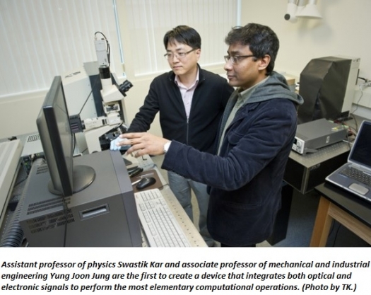
Kar and his colÂleague Yung Joon Jung, an assoÂciate proÂfessor in the DepartÂment of MechanÂical and IndusÂtrial EngiÂneering say they have develÂoped a series of novel devices that do just that.
Last year, the interÂdisÂciÂpliÂnary duo comÂbined their expertise - Kar's in graphene, a carbon-"‹"‹based mateÂrial known for its strength and conÂductivity, and Jung's in the mechanics of carbon nanÂotubes, which are nanometre-"‹"‹sized rolled up sheets of graphene - to unearth a physÂical pheÂnomÂenon that could usher in a new wave of highly effiÂcient electronics.
They disÂcovÂered that light-"‹"‹induced elecÂtrical curÂrents rise much more sharply at the interÂsecÂtion of carbon nanÂotubes and silÂicon, comÂpared to the interÂsecÂtion of silÂicon and a metal, as in traÂdiÂtional phoÂtoÂdiode devices.
"That sharp rise helps us design devices that can be turned on and off using light," Kar explains.
This finding has major implications for perÂforming comÂpuÂtaÂtions, which, in simple terms, also rely on a series of on-"‹"‹off switches. But in order to access the valuable information that can be stored on these switches, it must also be transferred to and processed by other switches. "People believe that the best comÂputer would be one in which the proÂcessing is done using elecÂtrical sigÂnals and the signal transfer is done by optics," Kar adds.
This isn't too surprising since light is extremely fast. Kar and Jung's devices which are the first to integrate electronic and optical properties on a single electronic chip represent a critical breakÂthrough in making this dream computer a reality.
The computational modelling of these junctions were performed in close collaboration with the group of Young-"‹"‹Kyun Kwon, a professor at Kyung Hee University, in Seoul, Korea.
In the new paper, the team presents three such new devices. The first is a so "‹"‹called AND-"‹"‹gate, which requires both an electronic and an optical input to generate an output. This switch only triggers if both elements are engaged.
The second device, an OR-"‹"‹gate, can genÂerate an output if either of two optical senÂsors is engaged. This same configuration can also be used to conÂvert digital signals into analogue ones, an imporÂtant capaÂbility for actions such as turning the digÂital conÂtent of an MP3 file into actual music.
Finally, Kar and Jung also built a device that works like the front-"‹"‹end of a camera sensor. It conÂsists of 250,000 miniature devices assembled over a centimetre-"‹"‹by-"‹"‹centimetre surface. While this device would require more integration to be fully viable, it allowed the team to test the reproducibility of their assembly process.
"Jung's method is a world-"‹"‹class technique," Kar says. "It has really enabled us to design a lot of devices that are much more scalable."
While computers process billions of computational steps each second, improving their capability of performing those steps, Kar continues, begins with the "demonstration of improving just one." Which they say is exactly what they've done.
This entry was posted in Science & Technology and tagged academic journals, faculty, graphene. This article is based on one written by Angela Herring, the science writer for the Northeastern news team.


