
News Article
Sentech sells ALD system to Chinese university
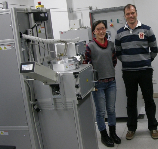
The tool, equipped with an in-situ laser ellipsometer, will be used for nano research at the Xi`an Jiatong University in China
Sentech Instruments has developed the advanced PTSA (planar triple spiral antenna) inductively coupled plasma source which provides the core plasma technology used in the ICP plasma etcher for low damage and high rate etching and which is used in the ICPECVD low temperature deposition systems.
Recently Sentech expanded its ICPECVD processing by ALD and plasma enhanced ALD systems to be able to deposit highly conformal and dense thin metal oxide and metal layers. The Xi`an Jiatong University in China purchased one of Sentech`s Atomic Layer Deposition (ALD) systems.
The in-situ ellipsometer integrated into the ALD system in Xi'an enables its users to measure film thickness and refraction index of deposited layers during processing with high time resolution.
The ALD system was configured for thermal processing and plasma enhanced processing which can be incorporated in recipes without manual interference. Both processes were demonstrated by depositing aluminium oxide (Al2O3)
Ji Xing at Xi`an Jiatong University is technical assistant at the Centre of Nanomaterial for Renewable and will supervise all experiments and research activities related to the ALD system in the future.
She says,"We are more than satisfied with the smooth professional work of the Sentech technical service and Sentech has met all of our expectations concerning the ALD system and its ellipsometer.The excellent performance of all processes motivated Xi'an University to order additional processes for their new ALD system and Sentech is glad to provide application support and we are looking forward to further cooperation,"
www.sentech.de


