
A new kind of electronics
A material based on strontium titanate could change the face of electronics
Researchers at the Vienna University of Technology claim they have created a stable two-dimensional electron gas in strontium titanate.
Usually, microelectronic devices are made of silicon or similar semiconductors.
Recently, the electronic properties of metal oxides have become quite interesting. These materials are more complex, yet offer a broader range of possibilities to tune their properties.

Zhicheng Zhong, Xianfeng Hao, Zhiming Wang, Stefan Gerhold (left to right)
An important breakthrough has now been achieved at the Vienna University of Technology.
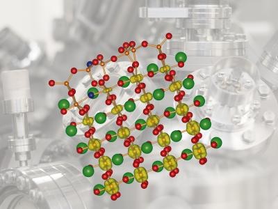
A two dimensional electron gas was created in strontium titanate (SrTiO3). In a thin layer just below the surface electrons can move freely and occupy different quantum states.

A Strontium-Titanoxide-crystal in the vacuum chamber
The scientists believe SrTiO3 could be a future alternative to standard semiconductors and also exhibit interesting phenomena, such as superconductivity, thermoelectricity or magnetic effects that do not occur in the materials that are used for today's electronic devices.
The Surface Layer and the Inside
This project closely links theoretical calculations and experiments. Zhiming Wang led the experiments. Some of the experimental work was done at the synchrotron BESSY in Berlin. Zhicheng Zhong from Karsten Held's group studied the material in computer simulations.
Not all of the atoms of strontium titanate are arranged in the same pattern: if the material is cut at a certain angle, the atoms of the surface layer form a structure, which is different from the structure in the bulk of the material.
"Inside, every titanium atom has six neighbouring oxygen atoms, whereas the titanium atoms at the surface are only connected to four oxygen atoms each," says Ulrike Diebold. This is the reason for the remarkable chemical stability of the surface. Normally such materials are damaged if they come into contact with water or oxygen.
Migrating Oxygen Atoms
Something remarkable happens when the material is irradiated with high-energy electromagnetic waves: "The radiation can remove oxygen atoms from the surface," Ulrike Diebold explains. Then other oxygen atoms from within the bulk of the material move up to the surface. Inside the material, an oxygen deficiency builds up, as well a surplus of electrons.
"These electrons, located in a two dimensional layer very close to the surface, can move freely. We call this an electron gas," says Karsten Held.
There has already been some evidence of two dimensional electron gases in similar materials, but until now the creation of a stable, durable electron gas at a surface has been impossible. The properties of the electrons in the gas can be finely tuned. Depending on the intensity of the radiation, the number of electrons varies. By adding different atoms, the electronic properties can also be changed.
"In solid state physics, the so-called band structure of a material is very important. It describes the relationship between the energy and the momentum of the electrons. The remarkable thing about our surface is that it shows completely different kinds of band structures, depending on the quantum state of the electron," continues Held.
The electron gas in the new material exhibits a multitude of different electronic structures. Some of them could very well be suitable for producing interesting magnetic effects or superconductivity. The promising properties of SrTiO3 will now be further investigated. The researchers hope that, by applying external electric fields or by placing additional metal atoms on the surface, the new material could reveal a few more of its secrets.


