
News Article
Enhancing power efficiency for future computer processors
A new class of magnetic materials called 'multiferroics.' could make future devices far more energy-efficient than current technologies
Have you ever wondered why your laptop or smartphone feels warm when you're using it? That heat is a byproduct of the microprocessors in your device using electric current to power computer processing functions and is actually wasted energy.
Now, a team led by researchers from the UCLA Henry Samueli School of Engineering and Applied Science has made major improvements in computer processing using an emerging class of magnetic materials called 'multiferroics.'
The researchers believe these advances could make future devices far more energy-efficient than current technologies. With today's device microprocessors, electric current passes through transistors, which are essentially very small electronic switches.
Because current involves the movement of electrons, this process produces heat which makes devices warm to the touch. These switches can also 'leak' electrons, making it difficult to completely turn them off. And as chips continue to get smaller, with more circuits packed into smaller spaces, the amount of wasted heat grows.
The UCLA Engineering team used multiferroic magnetic materials to reduce the amount of power consumed by 'logic devices,' a type of circuit on a computer chip dedicated to performing functions such as calculations. A multiferroic can be switched on or off by applying alternating voltage - the difference in electrical potential.
It then carries power through the material in a cascading wave through the spins of electrons, a process referred to as a spin wave bus.
A spin wave can be thought of as similar to an ocean wave, which keeps water molecules in essentially the same place while the energy is carried through the water, as opposed to an electric current, which can be envisioned as water flowing through a pipe, says principal investigator Kang L. Wang, UCLA's Raytheon Professor of Electrical Engineering and director of the Western Institute of Nanoelectronics (WIN).
"Spin waves open an opportunity to realise fundamentally new ways of computing while solving some of the key challenges faced by scaling of conventional semiconductor technology, potentially creating a new paradigm of spin-based electronics," Wang explains.
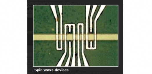
The image above shows a picture of spin wave devices, showing magneto-electric cells used for voltage-controlled spin wave generation in the spin wave bus material (yellow stripe). The yellow stripe is about four microns in diameter.
The UCLA researchers were able to demonstrate that using this multiferroic material to generate spin waves could reduce wasted heat and therefore increase power efficiency for processing by up to 1,000 times. Their research is published in the journal Applied Physics Letters.
"Electrical control of magnetism without involving charge currents is a fast-growing area of interest in magnetics research," says co-author Pedram Khalili, a UCLA assistant adjunct professor of electrical engineering. "It can have major implications for future information processing and data-storage devices, and our recent results are exciting in that context."
The researchers previously applied this technology in a similar way to computer memory.
The work is described in detail in the paper, "Electric-field-induced spin wave generation using multiferroic magnetoelectric cells," by Sergiy Cherepov et al in Appl. Phys. Lett. 104, 082403 (2014). doi:10.1063/1.4865916
The research was funded by the Defence Advanced Research Projects Agency's Non-Volatile Logic program and the by the Nanoelectronics Research Initiative through the WIN.
Now, a team led by researchers from the UCLA Henry Samueli School of Engineering and Applied Science has made major improvements in computer processing using an emerging class of magnetic materials called 'multiferroics.'
The researchers believe these advances could make future devices far more energy-efficient than current technologies. With today's device microprocessors, electric current passes through transistors, which are essentially very small electronic switches.
Because current involves the movement of electrons, this process produces heat which makes devices warm to the touch. These switches can also 'leak' electrons, making it difficult to completely turn them off. And as chips continue to get smaller, with more circuits packed into smaller spaces, the amount of wasted heat grows.
The UCLA Engineering team used multiferroic magnetic materials to reduce the amount of power consumed by 'logic devices,' a type of circuit on a computer chip dedicated to performing functions such as calculations. A multiferroic can be switched on or off by applying alternating voltage - the difference in electrical potential.
It then carries power through the material in a cascading wave through the spins of electrons, a process referred to as a spin wave bus.
A spin wave can be thought of as similar to an ocean wave, which keeps water molecules in essentially the same place while the energy is carried through the water, as opposed to an electric current, which can be envisioned as water flowing through a pipe, says principal investigator Kang L. Wang, UCLA's Raytheon Professor of Electrical Engineering and director of the Western Institute of Nanoelectronics (WIN).
"Spin waves open an opportunity to realise fundamentally new ways of computing while solving some of the key challenges faced by scaling of conventional semiconductor technology, potentially creating a new paradigm of spin-based electronics," Wang explains.
The image above shows a picture of spin wave devices, showing magneto-electric cells used for voltage-controlled spin wave generation in the spin wave bus material (yellow stripe). The yellow stripe is about four microns in diameter.
The UCLA researchers were able to demonstrate that using this multiferroic material to generate spin waves could reduce wasted heat and therefore increase power efficiency for processing by up to 1,000 times. Their research is published in the journal Applied Physics Letters.
"Electrical control of magnetism without involving charge currents is a fast-growing area of interest in magnetics research," says co-author Pedram Khalili, a UCLA assistant adjunct professor of electrical engineering. "It can have major implications for future information processing and data-storage devices, and our recent results are exciting in that context."
The researchers previously applied this technology in a similar way to computer memory.
The work is described in detail in the paper, "Electric-field-induced spin wave generation using multiferroic magnetoelectric cells," by Sergiy Cherepov et al in Appl. Phys. Lett. 104, 082403 (2014). doi:10.1063/1.4865916
The research was funded by the Defence Advanced Research Projects Agency's Non-Volatile Logic program and the by the Nanoelectronics Research Initiative through the WIN.


