
News Article
STATS ChipPAC flexible packaging set to enable 450mm
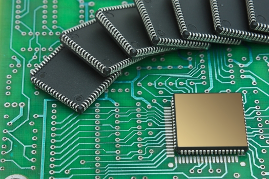
The firm says its FlexLine method is an approach to wafer level manufacturing that provides freedom from wafer diameter constraints
STATS ChipPAC has designed and implemented a new process that is a shift from conventional wafer level manufacturing.
The company says this approach, known as FlexLine, delivers flexibility and cost savings for wafer level packaging (WLP). With conventional WLP, an integrated circuit (IC) is fabricated, packaged and tested while still in a wafer format to streamline the manufacturing process.
WLP leverages the same semiconductor equipment infrastructure as wafer fabrication which is progressively more expensive for larger wafer diameters and finer silicon geometries.
The costs associated with transitioning to larger wafer diameters have resulted in extreme pricing pressures on WLP, particularly for mature technology such as wafer level chip scale packaging (WLCSP).
"Growing demand for WLCSP in a range of advanced mobile products, from low-cost to high-end smartphones and tablets, is driving capacity constraints in the industry, particularly with 200mm wafers. This is causing extreme pressure on our customers to weigh the high cost of transitioning to more advanced silicon nodes against the need to achieve dramatic cost reductions for more competitive end products," says Chong Khin Mien, Senior Vice President of Product and Technology Marketing, STATS ChipPAC.
"Capacity and cost challenges for WLCSP exist today in 200mm and 300mm wafer diameters and will inevitably intensify when the semiconductor industry transitions to 450mm wafers. This is an exciting time to drive a fundamental change in the manufacturing process for WLCSP," continues Chong Khin Mien.
STATS ChipPAC says its new FlexLine method is an approach to wafer level manufacturing that provides freedom from wafer diameter constraints while enabling supply chain simplification and significant cost reductions that are not possible with a conventional manufacturing flow.
"STATS ChipPAC is driving a significant paradigm shift in wafer level packaging with our FlexLine method. We have leveraged our proven reconstitution process, which has produced more than half a billion units of fan-out wafer level packages, to extend flexibility and cost advantages to fan-in WLCSP devices," says Han Byung Joon, Executive Vice President and Chief Technology Officer, STATS ChipPAC.
"We are the first company in the world to introduce a WLP method that is completely independent of incoming wafer sizes, including future 450mm wafer size, and delivers unprecedented flexibility in producing both fan-out and fan-in packages on the same manufacturing line," continues Han Byung Joon.
By normalising multiple wafer diameters to a uniform processing size through reconstitution, the original wafer diametres become irrelevant as this no longer dictates manufacturing capacity or limits process capabilities. When 200mm wafers are reconstituted into 300mm or larger panel sizes, customers have greater potential for cost reduction than conventional WLP manufacturing.
As the panel size increases, the cost of producing wafer level packages drops significantly when compared to conventional WLP methods.
Han Byung Joon concludes, "With FlexLine, we are able to help our customers achieve at least a 15 to 30 percent cost reduction using the optimum design requirements for their WLCSP devices. Later this year we will introduce unique technology enhancements to WLCSP that improve the reliability performance over WLCSPs produced with conventional methods. Our FlexLine method provides a strong manufacturing platform that enables future innovation in our wafer level packaging portfolio."


