
Optical patterned wafer inspection tool market to escalate
Research and Markets has announced the addition of the "Global Optical Patterned Wafer Inspection Equipment Market 2014-2018" report to its offerings.
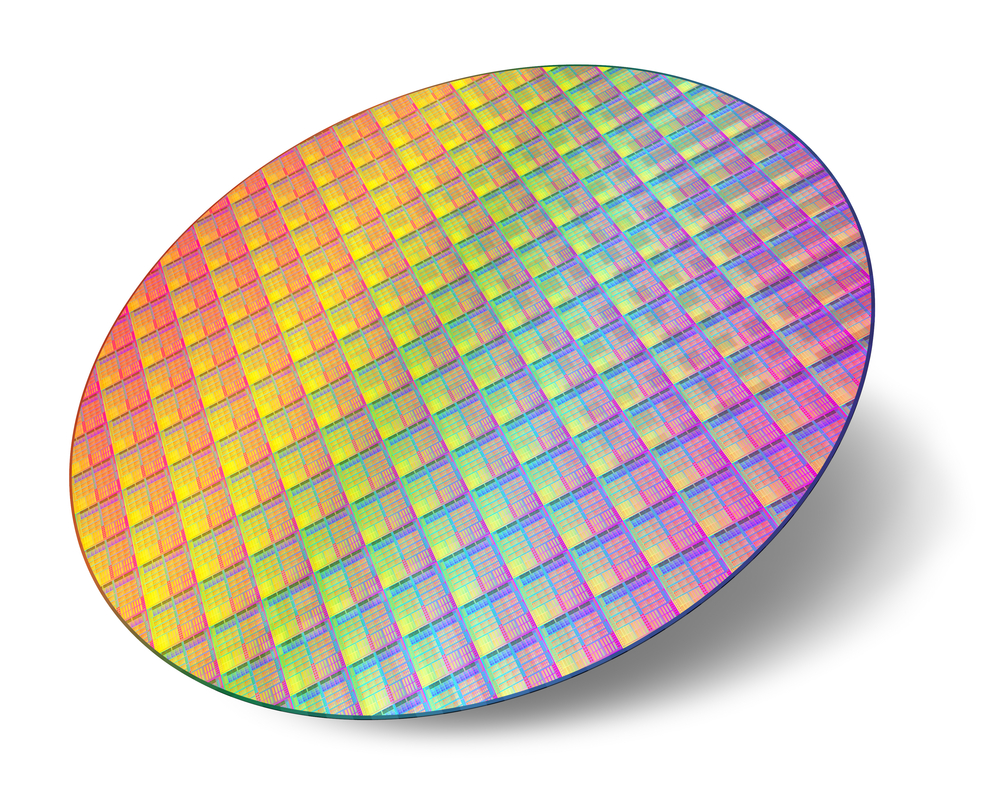
Optical patterned wafer inspection equipment is used to detect defects that occur during the semiconductor manufacturing processes.
The increasing complexity of semiconductor manufacturing due to new design rules and processes has increased the density of defects in the semiconductor wafers. This in turn can ruin an entire wafer rather than just a die.
Thus, optical patterned wafer inspection equipment is used by the semiconductor manufacturers to detect critical defects in semiconductor wafers. Optical patterned wafer inspection equipment helps the semiconductor manufacturers to effectively launch new products more quickly.
This is mainly because they can introduce stringent inspection equipment such as optical patterned wafer inspection equipment in their manufacturing process to prevent any defects in the final product.
The analysts forecast the Global Optical Patterned Wafer Inspection Equipment market to grow at a CAGR of 7.8 percent over the period 2013 to 2018.
The areas analysed include the Americas (USA), EMEA, and APAC (Taiwan).
Key vendors in this sector are Applied Materials and KLA Tencor while other prominent vendors are ASML, Hitachi High-technologies, JEOL , Tokyo Seimitsu, and Toray Engineering.
Commenting on the report, an analyst from the team says, "Rapid technological advancements such as transition from 300mm wafer to 450mm wafers, increasing adoption of FinFET architecture, emergence of 3D ICs, and introduction of 3D NAND architecture present a strong growth opportunity for optical patterned wafer inspection equipment. "
The analyst adds, "With the introduction of new technologies, the complexity of the semiconductor device also increases. This in turn paves the way for the use of inspection tools and equipment. Thus, it has become increasingly important for semiconductor inspection systems to ensure the reliability of semiconductors since semiconductors are expected to become more complex and advanced. This trend is expected to have a medium-term impact on the growth of the market over the next few years."


