+44 (0)24 7671 8970
More publications     •     Advertise with us     •     Contact us
 
News Article

Zeiss and NuFlare continue lithography collaboration

News

The development of mask writing and mask registration tools is a real enabler for the industry. Advances on both sides promote next generation lithography technologies such as Multi-Patterning, Directed Self-Assembly and EUV as well as EUV and 193i mix-and-match using cut masks

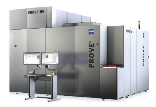
NuFlare Technology has approved factory specifications of its next generation mask metrology tool PROVE HR, pictured above. 

Zeiss' PROVE is said to enable the calibration of most advanced mask writing tools needed to support upcoming optical as well as next generation lithography technologies like EUV.

The system was shipped to Japan at the end of March.

The new PROVE HR is claimed to have a superior resolution realised by a redesigned beam path working with an NA of 0.8 at 193nm wavelength.

Fumiaki Shigemitsu, President of NuFlare Technology, Inc., says, "The achieved measurement results are beyond our expectations and allow us, to adjust even the smallest deflection fields in our e-beam tools for any remaining placement error. The much higher sampling of small features enables a better tool calibration of our e-beam writers."

Nuflare will use the Zeiss metrology tool to develop special calibration routines for the newest mask writer generations.

Oliver Kienzle, Managing Director of Carl Zeiss SMS GmbH highlights the benefits of the successful cooperation. He says, "The coherent development of mask writing and mask registration tools is a real enabler for the industry. The advances on both sides promote next generation lithography technologies such as Multi-Patterning, Directed Self-Assembly and EUV as well as EUV and 193i mix-and-match using cut masks. Therefore we are looking forward to extend our cooperation with NuFlare Technology in the future."

Purdue, imec, Indiana announce partnership
Resilinc partners with SEMI on supply chain resilience
NIO and NXP collaborate on 4D imaging radar deployment
Panasonic Industry digitally transforms with Blue Yonder
Global semiconductor sales decrease 8.7%
MIT engineers “grow” atomically thin transistors on top of computer chips
Keysight joins TSMC Open Innovation Platform 3DFabric Alliance
Leti Innovation Days to explore microelectronics’ transformational role
Quantum expansion
indie launches 'breakthrough' 120 GHz radar transceiver
Wafer fab equipment - facing uncertain times?
Renesas expands focus on India
Neuralink selects Takano Wafer Particle Measurement System
Micron reveals committee members
Avoiding unscheduled downtime in with Preventive Vacuum Service
NFC chip market size to surpass US$ 7.6 billion
Fujifilm breaks ground on new €30 million European expansion
Fraunhofer IIS/EAS selects Achronix embedded FPGAs
Siemens announces certifications for TSMC’s latest processes
EU Chips Act triggers further €7.4bn investment
ASE recognised for excellence by Texas Instruments
Atomera signs license agreement with STMicroelectronics
Gartner forecasts worldwide semiconductor revenue to decline 11% in 2023
CHIPS for America outlines vision for the National Semiconductor Technology Center
TSMC showcases new technology developments
Alphawave Semi showcases 3nm connectivity solutions
Greene Tweed to open new facility in Korea
Infineon enables next-generation automotive E/E architectures
Global AFM market to reach $861.5 million
Cepton expands proprietary chipset
Semtech adds two industry veterans to board of directors
Specialty gas expansion
×
Search the news archive

To close this popup you can press escape or click the close icon.
Logo
×
Logo
×
Register - Step 1

You may choose to subscribe to the Silicon Semiconductor Magazine, the Silicon Semiconductor Newsletter, or both. You may also request additional information if required, before submitting your application.


Please subscribe me to:


You chose the industry type of "Other"

Please enter the industry that you work in: