
News Article
Obducat reveals mass production lithography tool
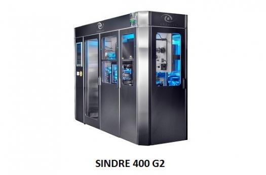
The system is capable of imprinting structure, with sizes ranging from 20nm and upwards, on substrate sizes up to 200 mm in diameter
Obducat, a manufacturer of lithography solutions based on nanoimprint lithography (NIL), has launched its 2nd generation SINDRE.
With the improved performance it will represent a cost effective NIL production solution on the market. The system is based on Obducat's patented SoftPress, IPS and STU technologies.
The fully automated SINDRE system enables throughputs of up to sixty wafers per hour.
The new SINDRE integrates the latest advances in manufacturing technology which enables high throughput, high repeatability at a defectivity level which surpass industry requirements.
The first system has already been delivered and passed customer final approval in January this year and the next system will be delivered in third quarter this year.
The new SINDRE platform is a fully integrated NIL system which includes integrated fabrication of the Intermediate Polymer Stamp (IPS). This is a proven and reliable process which was also integrated in previous generation of SINDRE systems delivered by Obducat during the last five years.
Obducat's patented IPS technology covers the use of a transparent flexible stamp in any kind of imprint process. The use of the IPS technology ensures a long life time of the stampers which minimise the stamp related costs per imprint.
The patented SoftPress technology, applied in the system, ensures the necessary level of conformity between the stamp and substrate vital for establishing high imprint uniformity. This enables a large process window for downstream processes leading to a high yield and low Cost of Ownership. All this has been integrated into a very compact system having a small footprint.
The new SINDRE system also offers a wide flexibility which includes the possibility to use different resists and IPS materials to support customisation of the imprint process. In addition the system can run both UV as well as thermal based NIL processes, giving the capability to imprint structure sizes ranging from 20nm and upwards, on substrate sizes up to 200 mm in diameter.
"The versatility and superior performance of our patented key technologies has been extended further to safeguard Obducat's continued technological leadership in the NIL industry," says Babak Heidari, CTO of Obducat.
Example of components which are ideally produced with this system are optical, photonic, LEDs, fluidic and other biomedical components.
"Obducat again confirms its leading position with this launch. With more than 130 NIL systems delivered during the last decade and several of these being used for manufacturing purposes in LEDs, photonics and biomedical applications, we are breaking new barriers in terms of performance and cost efficiency," finishes Patrik Lundström, CEO of Obducat.


