
STS Semi and Invensas to push bonding for mobile solutions
Invensas, a wholly owned subsidiary of Tessera, and STS Semiconductor & Telecommunications have entered into an agreement to validate high volume manufacturing capability for Invensas' patented Bond Via Array (BVA) technology for next generation smartphone and tablet customers.
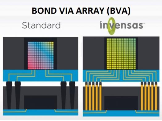
BVA is a Package-on-Package (PoP) technology for System on Chip (SOC) and memory integration in mobile devices.
Styled as a "Bridge Technology to 3DIC", solution, it utilises established wire-bond assembly techniques to enable low power and high-bandwidth (1000 IO+) packaging in an ultra-small form factor, ideal for mobile devices. STS's engineering and high-volume capabilities provide a suitable platform for high volume manufacturing of BVA.
"We are delighted to partner with Invensas on BVA," says Chang-Bum Shim, Chief Operating Officer and Executive Vice President for STS. "STS understands the critical need to increase interconnect bandwidth for the growing Package-on-Package mobile SOC market, without increasing product size or the cost to the end user. Our engineering and manufacturing capabilities are ideally suited to the commercialisation of BVA."
"STS is an ideal partner for BVA," Simon McElrea, CTO of Tessera Technologies, Inc. and President of Invensas, comments. "Their continual investment in cutting-edge packaging technology and associated manufacturing capability, coupled with their growth model in mobile and communication devices, is perfectly aligned for BVA commercialisation."


