
Spasers could bring mobiles to T-shirts
Spaser-based devices could provide an alternative to transistor-based devices such as microprocessors, memory, and displays
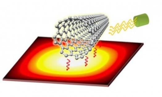
A team of researchers from Monash University's Department of Electrical and Computer Systems Engineering (ECSE) has modelled the world's first spaser (surface plasmon amplification by stimulated emission of radiation) to be made completely of carbon.
A spaser is effectively a nanoscale laser or nanolaser. It emits a beam of light through the vibration of free electrons, rather than the space-consuming electromagnetic wave emission process of a traditional laser.
PhD student and lead researcher Chanaka Rupasinghe says the modelled spaser design using carbon would offer many advantages.
"Other spasers designed to date are made of gold or silver nanoparticles and semiconductor quantum dots while our device would be comprised of a graphene resonator and a carbon nanotube gain element," Rupasinghe explains.
"The use of carbon means our spaser would be more robust and flexible, would operate at high temperatures, and be eco-friendly.Because of these properties, there is the possibility that in the future an extremely thin mobile phone could be printed on clothing."
Spaser-based devices can be used as an alternative to current transistor-based devices such as microprocessors, memory, and displays to overcome current miniaturising and bandwidth limitations.
The researchers chose to develop the spaser using graphene and carbon nanotubes. They are more than a hundred times stronger than steel and can conduct heat and electricity much better than copper. They can also withstand high temperatures.
The scientists say their research showed, for the first time, that graphene and carbon nanotubes can interact and transfer energy to each other through light. These optical interactions are very fast and energy-efficient, and so are suitable for applications such as computer chips.
"Graphene and carbon nanotubes can be used in applications where you need strong, lightweight, conducting, and thermally stable materials due to their outstanding mechanical, electrical and optical properties. They have been tested as nanoscale antennas, electric conductors and waveguides," Rupasinghe notes.
Rupasinghe says a spaser generated high-intensity electric fields concentrated into a nanoscale space. These are much stronger than those generated by illuminating metal nanoparticles by a laser in applications such as cancer therapy.
"Scientists have already found ways to guide nanoparticles close to cancer cells. We can move graphene and carbon nanotubes following those techniques and use the high concentrate fields generated through the spasing phenomena to destroy individual cancer cells without harming the healthy cells in the body," concludes Rupasinghe.
This work has been published in the paper, "Spaser Made of Graphene and Carbon Nanotubes," by Chanaka Rupasinghe et al in ACS Nano, 2014, 8 (3), pp 2431"“2438. DOI: 10.1021/nn406015d


