
Toshiba shipping samples of embedded NAND Flash memory modules
The JEDEC UFS Ver.2.0 standard compliant embedded memories combine up to 64GB NAND and a controller in a single package
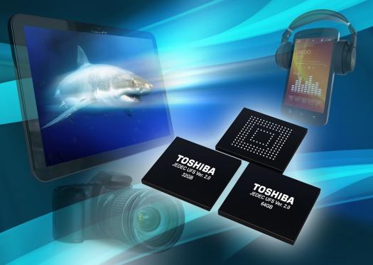
Toshiba Electronics Europe has started sample shipments of 32-gigabyte and 64-gigabyte (GB) embedded NAND Flash memory modules compliant with the JEDEC UFS Ver.2.0 standard.
According to a Toshiba survey in April 2014 for embedded NAND Flash memory modules, the firm claims it is the first company in the industry to do so.
Universal Flash Storage (UFS) is a product category for a class of embedded memory products built to the JEDEC UFS standard specification.
The product supports maximum transfer rates up to 11.6Gbps by integrating two 5.8Gbps High-speed MIPI M-PHYHS-G3 I/F data lanes - an optional feature of UFS Ver. 2.0.
The modules achieve ultra-high read/write performance with read speeds reaching 650MB/s and write speeds reaching 180MB/s. The faster transfer speeds can shorten the time taken to launch many kinds of applications, shoot digital still images, and play and download large data movie and music files on mobile products like smartphones or tablets.
The modules are sealed in a small 153 ball FBGA package measuring just 11.5mm x 13.0mm x 1.0mm for the 32GB die and 11.5mm x 13.0mm x 1.2mm for the 64GB die and have a signal layout compliant with JEDEC UFS Ver.2.0. The modules are rated for an operating temperature of -25°C to +85°C and support memory core voltages of 2.7V to 3.6V.
Demand continues to grow for large density, high-performance chips that support high resolution video, driven by improved data-processing speeds in host chipsets and wider bandwidths for wireless connectivity in a wide range of digital consumer products, including smartphones and tablet PCs.
The JEDEC UFS Ver.2.0 compliant interface handles essential functions, including writing block management, error correction and driver software. It simplifies system development, allowing manufacturers to minimize development costs and speed up time to market for new and upgraded products.
Toshiba says it is is now reinforcing its position in this area by being the first in the industry to deliver samples with a high performance UFS module.
Toshiba will schedule mass production and add other densities to the line-up in response to market demand.


