
New NIST FIB microscope doesn't lie
A new microscope could provide a process for stencilling patterns on silicon chips. The technique requires etching into the silicon through the spaces in the lithography stencil to transfer the pattern
The limitations of microscopes affect the truths they can tell. For example, scanning electron microscopes (SEMs) just can't see materials that don't conduct electricity very well, and their high energies can actually damage some types of samples.
In an effort to extract a little more truth from the world of nanomaterials and nanostructures, researchers at the National Institute of Standards and Technology (NIST) have built what they say is the first low-energy focused ion beam (FIB) microscope that uses a lithium ion source.
The team's new approach opens up the possibility of creating a whole category of FIBs using any one of up to twenty different elements, greatly increasing the options for imaging, sculpting, or characterising materials.
Although the new microscope's resolution isn't yet as good as a SEM or a helium ion microscope (HIM), it can image nonconductive materials and can more clearly visualise the chemical composition on the surface of a sample than the higher-energy SEMs and FIBs.
And, by analysing the energy with which the ions scatter, the researchers have shown that the microscope should be able to not only see that adjacent materials are chemically different, but also identify the elements that make them up.
Jabez McClelland and his colleagues at NIST applied Nobel Prize-winning laser cooling techniques to make the first low-energy FIB using lithium ions in 2011. Since then, they have been working to refine the technique to increase the beam's brightness and collimation, i.e., getting all the ions to move in the same direction to make it more useful for imaging applications.
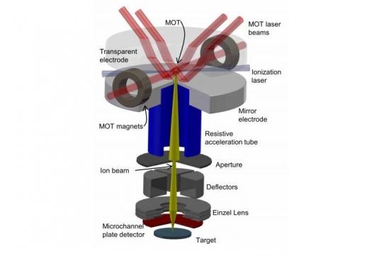
The new instrument, pictured at the top of this story, first cools a gas of neutral lithium atoms to a temperature of about 600 microkelvins, just a few millionths of a degree above absolute zero. To do this, it uses lasers and a magneto-optical trap (MOT) to hold the atoms. Another laser ionises the atoms and then electric fields accelerate them, straightening out their flight and focusing the beam on a target.

Micrographs of a spot of electronics solder demonstrate how the lithium FIB microscope (left) clearly distinguishes between the lead and tin components. An SEM image (right) captures mainly topological differences. Images show a region approximately 28 microns across (Credit: Twedt/CNST)
The NIST FIB can produce lithium ion beams with energies in the range of 500 electron volts to 5,000 electron volts (compared to about30,000 electron volts for HIMs.) The NIST team can reduce the beam's energy even further, but repulsive interaction effects at the source limit how small they can focus the beam when the accelerating field is weaker.
As detailed in their paper, the team demonstrated how their microscope could help to solve a common problem in nanoimprint lithography, a process for stencilling patterns on silicon chips. This technique requires etching into the silicon through the spaces in the lithography stencil to transfer the pattern.
"Before manufacturers can etch the silicon, they have to make sure the spaces are free of chemical residue," says McClelland. "Commonly, they use a process called plasma etching to clean that residue off, but they have to be careful not to overdo it or they can damage the substrate and ruin the chip. Our FIB scope could check to see if the plasma has done its work without damaging the chip. A scanning electron microscope couldn't do this because it's difficult to see the thin residue, and the high-energy beam is likely to charge up and/or melt the stencil and make the problem worse."
The group has big plans for the microscope. One future project they're planning to do is trying to unravel exactly how lithium batteries work by injecting lithium ions into the materials and watching how they affect the behaviour of the batteries. This and other applications will add to the capabilities of NIST's nanotechnology user facility, the Centre for Nanoscale Science and Technology, where the work is being carried out
A few former members of the group have started their own company to develop a low-energy caesium FIB for milling and sculpting features on the order of single nanometres, a huge leap in nanofabrication if successful.
"This new form of microscopy we've developed promises to provide a new tool for nanotechnology with good surface sensitivity, elemental contrast and high resolution," says McClelland. "The applications range from nanofabrication process control to nanomaterial development and imaging of biomaterials."
This work is described in the paper, "Scanning ion microscopy with low energy lithium ions," by K.A. Twedt et al in Ultramicroscopy, 142, July 2014, p24.


