
Toshiba to Replace Fab 2 for Transition to 3D NAND Tech
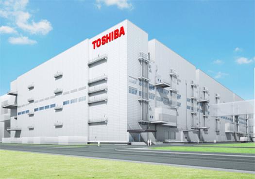
Toshiba Corporation has announced that it will demolish the No. 2 semiconductor fabrication facility (Fab 2) at Yokkaichi Operations, the company's NAND Flash memory plant in Mie prefecture, Japan, and replace it with a new fab on the same site.
Toshiba also entered into a non-binding memorandum of understanding with SanDisk Corporation to invest jointly in the new facility. The primary purpose of the new wafer fab is to secure space for converting existing Toshiba and SanDisk 2D NAND capacity to 3D NAND beginning in 2016.
Demolition work on the current Fab 2 will start in May with construction beginning in September 2014, with a target completion date of Summer 2015. The clean room within the new fab will be built in phases to align the clean room investment with the timing of conversion of 2D NAND capacity to 3D NAND. Construction of the initial cleanroom will be complete in time for 2016 output. Decisions on capacity conversion ramp and equipment investment, the start of production, and production levels in the new fab will reflect market trends.
The new fab will provide a supplementary facility for processes mainly dedicated to 3D NAND memory production, and work in close cooperation with Yokkaichi's other facilities. Toshiba and SanDisk will support 3D memory production with leading-edge manufacturing equipment for lithography, deposition and etching through joint ventures.
Yasuo Naruke, Corporate Senior Vice President of Toshiba Corporation and President and CEO of Semiconductor & Storage Products Company, said, "Our determination to develop advanced technologies underlines our commitment to respond to continued demand of NAND flash memory. We are confident that our joint venture with SanDisk will allow us to produce cost competitive next generation memories at Yokkaichi. "
Sanjay Mehrotra, President and Chief Executive Officer of SanDisk, said: "We are pleased to continue our long-standing collaboration with Toshiba in this new wafer fab, which will advance our leadership in memory technology into the 3D NAND era."
The new fab will have a quake absorbing structure and an environmentally friendly design that includes LED lighting throughout the building. It will also be equipped with the latest energy saving manufacturing equipment, which will secure productivity advances while lowering power consumption. Highly efficient use of waste heat will help to lower fuel consumption and cut CO2 emissions by 15% compared to Fab 5, currently the most advanced fab on the Yokkaichi site.
Toshiba and SanDisk will, through joint ventures, maximize investment efficiency in the transition to 3D NAND by making full use of the Yokkaichi site. Going forward, the companies will continue to jointly develop advanced process technology, and make investments to meet market requirements.


