
News Article
Ziptronix and EV Group Demonstrate Submicron Accuracies for Wafer-to-Wafer Hybrid Bonding
Ziptronix Inc. and EV Group ("EVG") have announced they have successfully achieved submicron post-bond alignment accuracy on customer-provided 300mm DRAM wafers.
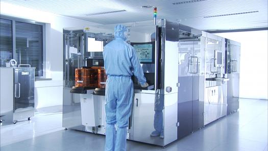
The results were achieved by implementing Ziptronix's DBI Hybrid Bonding technology on an EVG Gemini FB production fusion bonder and SmartView NT bond aligner. This approach can be used to manufacture fine-pitch 3D ICs for a variety of applications including stacked memory, advanced image sensors and stacked systems-on-chip (SoCs).
"The performance of DBI Hybrid Bonding technology is not limited by connection pitch, but requires the right alignment and placement tool with an ability to scale that has been a challenge to find until now," said Paul Enquist, CTO and VP Engineering at Ziptronix. "EVG's fusion bonding equipment has been optimized to achieve consistent submicron post-bond alignment accuracy. This advancement in alignment accuracy provides a clear path to high-volume manufacturing (HVM) of our technology."
Pitch scaling on next-generation 3D technologies is expected to continue for many years to come. Fine-pitch hybrid bonding is already in use in high-performance 3D memory products, and has been announced for HVM of 3D image sensors. DBI Hybrid Bonding can be used at the die or wafer level; however, wafer-level bonding enables a great cost benefit by bonding all the die at once. With much of the processing for DBI Hybrid Bonding taking place at wafer scale, there is the added benefit of low cost-of-ownership.
"Demonstrating submicron accuracy is critical to achieving fine-pitch connections in HVM for a wider variety of applications," said Paul Lindner, Executive Technology Director at EVG. "As the industry pushes to realize 3D ICs, joint efforts such as our work with Ziptronix to develop manufacturing approaches offer customers a tremendous value-add."
Ziptronix Direct Bond Interconnect (DBI) Hybrid Bonding is a conductor/dielectric bonding technology that includes a variety of metal/oxide and/or nitride combinations, does not use adhesives and is currently the most suitable for volume manufacturing in the marketplace. It allows for strong, room temperature dielectric bonding, low temperature conductive bonding and finer-pitch interconnect over Cu/Cu or other metal bonding because the bond occurs between both the dielectric and the conductive surfaces, which effectively bonds the entire substrate interface area.
EVG's SmartViewNT Automated Bond Alignment System for Universal Alignment offers a proprietary method of face-to-face wafer-level alignment, which is key to achieving the required accuracy in multiple wafer stacking for leading-edge technologies. In addition to improving alignment capabilities on its SmartView NT bond aligner to reach submicron accuracies, EVG has optimized it so that surfaces can be prepared simultaneously for bonding, electrical connectivity and mechanical strength.


