
Cheaper vertical 3D chip integration with AMAT tool
The Endura Ventura PVD system will allow high aspect ratio TSV structures for copper interconnects and is claimed to reduce cost of ownership by up to 50 percent
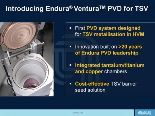
Applied Materials has launched the Endura Ventura PVD system that helps customers reduce the cost of fabricating smaller, lower power, high-performance integrated 3D chips.
The system incorporates Applied's latest developments in Physical Vapour Deposition (PVD) technology that enables the deposition of thin, continuous barrier and seed layers in through-silicon-vias (TSVs).

The Ventura system also supports the use of lower cost.titanium in volume production as an alternative barrier material..
With the launch of the Ventura system, Applied is expanding its toolset for wafer level packaging (WLP) applications, including TSVs, redistribution layer (RDL) and under bump metallisation (this is used to connect the die to substrate).
TSVs are a critical technology for vertically fabricating smaller and lower power future mobile and high-bandwidth devices. Vias are short vertical interconnects that pass through the silicon wafer, connecting the active side of the device to the back side of the die, providing the shortest interconnect path between multiple chips.
Integrating 3D stacked devices requires greater than 10:1 aspect ratio TSV interconnect structures to be metallised with copper. AMAT says the new Ventura tool solves this challenge with innovations in materials and deposition technology to manufacture TSVs more cost-effectively than previous industry solutions.
"These innovations deliver a higher-performance and more functional, yet, compact chip package with less power consumption to meet leading-edge computing needs. Customers are realising the benefits of this new PVD system and are qualifying it for volume manufacturing."

Supporting the manufacture of high-yielding 3D chips, the Ventura system introduces advances in ionised PVD technology that assure the integrity of the barrier and seed layers that are critical to superior gap-fill and interconnect reliability.
These developments are said to significantly improve ion directionality to enable the deposition of thin, continuous and uniform metal layers deep into the vias to achieve the void-free fill necessary for robust TSVs. With the improvement in directionality, higher deposition rates can be achieved, while the amount of barrier and seed material needed can be reduced.
These attributes of the Ventura system and the adoption of titanium as an alternate barrier are expected to improve device reliability and reduce the overall cost of ownership for TSV metallisation.


