+44 (0)24 7671 8970
More publications     •     Advertise with us     •     Contact us
 
News Article

Semiconductor engineering and fabrication expert joins Noel

News

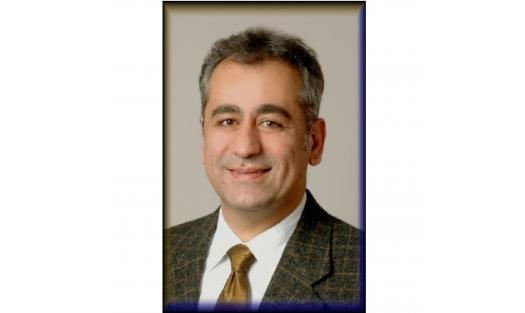
Noel Technologies, a Silicon Valley specialty foundry offering process development and substrate fabrication, has added semiconductor industry veteran Siavash Parsa to its growing management staff.

Parsa will manage and direct all aspects of Noel's process development, integration and fabrication.

Beyond his responsibilities in photolithography, Parsa will also direct technology in thin films, wet and dry etch, and wet and dry cleaning. He will manage the implementation of Noel's efforts in deep silicon etching with new, advanced etchers.

Recently, Noel announced its cost reduction processes for nanoimprint stamps. Parsa will continue enabling nanoimprint capabilities and also Noel's emphasis on working with MEMS and LED suppliers.

Parsa brings to Noel over twenty years of semiconductor engineering and fabrication management experience.

Most recently he was Process Engineering Manager for the University of California's Marvell Nanofabrication lab (formerly Microlab). There he was the project lead for the relocation of the entire operation (over 130 tools) to a new clean room lab. Prior to that he served in a number of engineering, photolithography, and fabrication management positions for several semiconductor manufacturers, including Xicor and Integrated Device Technology.

Purdue, imec, Indiana announce partnership
Resilinc partners with SEMI on supply chain resilience
NIO and NXP collaborate on 4D imaging radar deployment
Panasonic Industry digitally transforms with Blue Yonder
Global semiconductor sales decrease 8.7%
MIT engineers “grow” atomically thin transistors on top of computer chips
Keysight joins TSMC Open Innovation Platform 3DFabric Alliance
Leti Innovation Days to explore microelectronics’ transformational role
Quantum expansion
indie launches 'breakthrough' 120 GHz radar transceiver
Wafer fab equipment - facing uncertain times?
Renesas expands focus on India
Neuralink selects Takano Wafer Particle Measurement System
Micron reveals committee members
Avoiding unscheduled downtime in with Preventive Vacuum Service
NFC chip market size to surpass US$ 7.6 billion
Fujifilm breaks ground on new €30 million European expansion
Fraunhofer IIS/EAS selects Achronix embedded FPGAs
Siemens announces certifications for TSMC’s latest processes
EU Chips Act triggers further €7.4bn investment
ASE recognised for excellence by Texas Instruments
Atomera signs license agreement with STMicroelectronics
Gartner forecasts worldwide semiconductor revenue to decline 11% in 2023
CHIPS for America outlines vision for the National Semiconductor Technology Center
TSMC showcases new technology developments
Alphawave Semi showcases 3nm connectivity solutions
Greene Tweed to open new facility in Korea
Infineon enables next-generation automotive E/E architectures
Global AFM market to reach $861.5 million
Cepton expands proprietary chipset
Semtech adds two industry veterans to board of directors
Specialty gas expansion
×
Search the news archive

To close this popup you can press escape or click the close icon.
Logo
×
Logo
×
Register - Step 1

You may choose to subscribe to the Silicon Semiconductor Magazine, the Silicon Semiconductor Newsletter, or both. You may also request additional information if required, before submitting your application.


Please subscribe me to:


You chose the industry type of "Other"

Please enter the industry that you work in: