
Fraunhofer IPMS enhances ultrasonic sensors
Scientists at Fraunhofer Institute for Photonic Microsystems (IPMS) in Dresden have been using their experience in MEMS technologies to fabricate Capacitive Ultrasonic Micromachined Transducers (CMUTs).
CMUTs can send and receive ultrasound in an energy efficient manner, are environmentally friendly, provide miniaturisation capabilities, and expand the applications of ultrasound beyond today's state of the art.
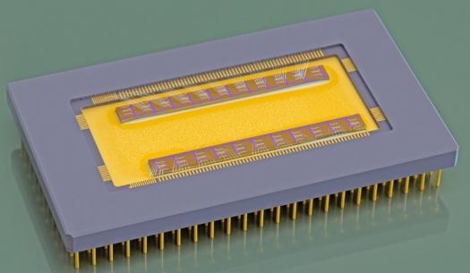
The image at the top of this story shows a CMUT chip on a ceramic carrier
Ultrasonic sensors have already become an integral part of our everyday lives. They support car drivers as parking aid, control filling levels and material flows in the food and beverage industry and enable medical imaging tools, such as foetal imaging and organic tissue imaging.
This versatile sensing principle is based on the propagation and evaluation of high frequency sound pulses, and enables contactless detection of objects with millimetric precision for a wide variety of materials regardless of their state, form and colour, and in practically any environment.
Today's ultrasonic transducers are typically manufactured using piezoelectric materials and have proven to be successful in many applications.
"CMUTs are not intended to replace these, but rather complement them and open up new fields of application for ultrasonic technology," stresses Anartz Unamuno, manager of the CMUT activities at Fraunhofer IPMS.
Several designs of CMUTs have been developed at the institute covering the frequency range between one and 50 megahertz.
Unamuno explains, "CMUTs are basically MEMS structures consisting of two opposing electrodes. One of the electrodes is static and the other deflectable. There is an insulating layer and a gap between the two electrodes. As an emitter, an electric signal is applied between the electrodes which deflects the movable electrode and generates an acoustic wave. The inverse energy transformation, acoustic to electric, is used with CMUTs to sense ultrasound waves".
Microelectronic technologies such as surface micromachining or wafer bonding processes are used for the fabrication of CMUTs, enabling a monolithic integration of the CMUTs with CMOS ASICs. Also, CMUTs provide greater sensitivity and broader frequency ranges than the established piezo based transducers.
Fraunhofer IPMS offers many years of experience in the pilot fabrication of MEMS components and the integration of MEMS on CMOS products. Unamuno intends to use this know-how together with his team in order to achieve a commercial breakthrough for CMUTs.
The first generation of CMUT arrays realised at Fraunhofer IPMS has already been characterised using electric and optic techniques.
Their acoustic performance has also been evaluated. The results will be presented to the public at the Sensors Expo to be held from June 24th to 26th, 2014 in the Donald E. Stephens Convention Centre Rosemont, Illinois. Here, a demonstrator will also show the functionality of a CMUT transducer in fluids. Visitors can find the exhibit at the Fraunhofer IPMS booth #421.


