
X-FAB first to buy LatticeAx 300 cleaving tool
LatticeGear has shipped the first of its new LatticeAx 300 cleaving systems to X-FAB Silicon Foundries, an analogue and mixed signal specialty foundry based in Erfurt, Germany.
According to Ekkehart Brandstädt, X-FAB's failure analysis team leader, "The LatticeAx is filling our need for cleaving accuracy and repeatability that goes beyond what can be achieved manually. It is less expensive, yet provides higher throughput, than automated microcleaving".
"With LatticeAx, which we often use for MEMS wafers with complicated structures, our lab is processing more cross-sections while using the lower throughput, automated microcleaver for jobs that require sub-micron accuracy. The introduction of the LatticeAx into our workflow has improved the total productivity and reduced the cost-per-cleave in our failure analysis lab," adds Brandstädt.
Manufacturers of semiconductors, solar cells, MEMS and other microelectronic devices need cross-section samples with high accuracy and quality for imaging in a scanning electron microscope (SEM).
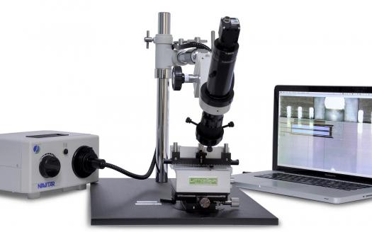
Manual approaches, which use a scribe mark to initiate the cleave, are fast and inexpensive, but offer limited accuracy and reliability. Automated systems with image processing and robotics can cleave to sub-micron accuracy, but are expensive, slow and pose many sample restrictions. The LatticeAx 300 (pictured at the top of this article) delivers ten-micrometre placement accuracy in five minutes at a fraction of the cost of automated systems.
LatticeGear's Efrat Moyal, Co-founder, states, "The key to the accuracy and quality of LatticeAx 300 is the integration of the controlled indentation and cleaving process with an advanced vision package and precise movement in X/Y.
A manual scribe mark is essentially a scratch, and on the microscopic level, it is composed of many micro fractures that can initiate cleaves in slightly different locations and directions. The LatticeAx micro indenter uses a precisely-controlled shape and pressure to initiate an accurate, predictable, high-quality cleave.
Efrat adds, "We complete the cleave by applying carefully-controlled pressure to the wafer. You can actually hear the cleave progress as it splits the wafer "“ very different from the sharp crack you hear with a manual cleave. We have even made very high-quality cleaves in non-crystalline substrates, such as glass, which we can only attribute to the repeatability and control of the indenting and cleaving process."


