
News Article
Samsung takes SSDs into the 3rd dimension
Samsung Electronics has launched the 850 PRO, a new solid state drive (SSD) line-up featuring Samsung's 3D vertical NAND (V-NAND) Flash memory technology. Samsung says its 850 PRO, unveiled at the 2014 Samsung SSD Global Summit in Seoul, offers a new breed of performance for solid state drives and will be available globally across 53 markets from this month.
Just how is Samsung V-NAND Flash memory able to offer a hundred times the capacity in only a tenth of the same area? That's where the V in V-NAND comes in, as Samsung stacks the cells vertically. Samsung's 3D V-NAND breaks free of the scaling limit for existing NAND Flash technology. Problems with Shrinking Technology Shrinking is a fundamental technological advancement in almost any field, but it gains significant importance in memory engineering. As memory structures shrink, so do the multitude of mobile devices people worldwide use on a daily basis. Samsung has committed considerable resources and effort toward researching and developing shrinking advancements while also working to mitigate the two biggest problems inherent in shrinking technology. These are dedcribed below.
Cell-to-Cell Interference When an electric charge flows into one cell, an electric charge flows into a neighbouring cell (known as the coupling effect). This extraneous charge to the neighbouring cell actually changes the stored data, resulting in corruption of that data. This interference does not occur when the space between cells is greater than 30nm, but as that space shrinks smaller than 20nm, the chance for cell-to-cell interference increases. Patterning Patterning is a manufacturing technology developed for photolithography to enhance density. The patterning process allows for geometries half as wide as the scanner is capable of printing, but it has its limits within the 10nm process range. Overcoming Inherent Shrinking Problems Samsung has developed and applied a variety of technologies to prevent both data-corrupting interference and the limits of patterning. 3D V-NAND replaces 2D Planar NAND's conductor with an insulator that allows cells to hold their charges after writing data. Due to its vertical cell arrangement, Samsung's 3D V-NAND features a wider bit line, effectively removing cell-to-cell interference. Stacking the vertical layers in three dimensions allowed for 24-layer products in 2013 and increased to 32-layer products in June 2014. Using stacking instead of photolithography to increase capacity eliminated the patterning limitation. "With the new 850 PRO V-NAND SSD, Samsung is introducing the next major evolution of SSD technology, taking the lead in delivering high-density SSDs with outstanding endurance, performance and energy efficiency," says Unsoo Kim, senior vice president of branded product marketing team at Samsung Electronics. "We are fully committed to establishing an innovative computing environment by providing customers with leading-edge V-NAND SSDs with unrivalled performance." According to Samsung, its 850 PRO delivers super-fast speeds and exceptional endurance, offering the highest level of performance among SSDs using the SATA III (6Gb/s) interface. Its sequential read performance reaches up to 550 megabytes per second (MB/s), with write performance of up to 520MB/s. Random read performance is up to 100,000 input/output operations-per-second (IOPS), with write speeds of up to 90,000 IOPS. The drive also offers a Dynamic Thermal Guard feature, which maintains ambient temperature while operating and prevents potential data loss from overheating. The Samsung 850 PRO will be available in 128 gigabyte (GB), 256GB, 512GB and 1 terabyte (TB) storage capacities. With the accelerating consumer adoption of SSDs, Samsung anticipates that its new V-NAND SSDs will add to the growth of the branded SSD market with its outstanding performance. According to the April 4th, 2014, "Gartner Forecast Analysis: NAND, Worldwide, 1Q14 Update," the global SSD market is expected to rapidly increase from US $11.04 billion in revenues in 2013 to approximately US $14.47 billion in 2014 and US $23.54 billion in 2017.
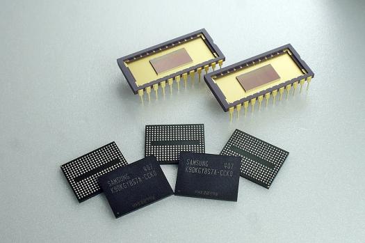
Samsung 850 PRO SSD
Just how is Samsung V-NAND Flash memory able to offer a hundred times the capacity in only a tenth of the same area? That's where the V in V-NAND comes in, as Samsung stacks the cells vertically. Samsung's 3D V-NAND breaks free of the scaling limit for existing NAND Flash technology. Problems with Shrinking Technology Shrinking is a fundamental technological advancement in almost any field, but it gains significant importance in memory engineering. As memory structures shrink, so do the multitude of mobile devices people worldwide use on a daily basis. Samsung has committed considerable resources and effort toward researching and developing shrinking advancements while also working to mitigate the two biggest problems inherent in shrinking technology. These are dedcribed below.
Cell-to-Cell Interference When an electric charge flows into one cell, an electric charge flows into a neighbouring cell (known as the coupling effect). This extraneous charge to the neighbouring cell actually changes the stored data, resulting in corruption of that data. This interference does not occur when the space between cells is greater than 30nm, but as that space shrinks smaller than 20nm, the chance for cell-to-cell interference increases. Patterning Patterning is a manufacturing technology developed for photolithography to enhance density. The patterning process allows for geometries half as wide as the scanner is capable of printing, but it has its limits within the 10nm process range. Overcoming Inherent Shrinking Problems Samsung has developed and applied a variety of technologies to prevent both data-corrupting interference and the limits of patterning. 3D V-NAND replaces 2D Planar NAND's conductor with an insulator that allows cells to hold their charges after writing data. Due to its vertical cell arrangement, Samsung's 3D V-NAND features a wider bit line, effectively removing cell-to-cell interference. Stacking the vertical layers in three dimensions allowed for 24-layer products in 2013 and increased to 32-layer products in June 2014. Using stacking instead of photolithography to increase capacity eliminated the patterning limitation. "With the new 850 PRO V-NAND SSD, Samsung is introducing the next major evolution of SSD technology, taking the lead in delivering high-density SSDs with outstanding endurance, performance and energy efficiency," says Unsoo Kim, senior vice president of branded product marketing team at Samsung Electronics. "We are fully committed to establishing an innovative computing environment by providing customers with leading-edge V-NAND SSDs with unrivalled performance." According to Samsung, its 850 PRO delivers super-fast speeds and exceptional endurance, offering the highest level of performance among SSDs using the SATA III (6Gb/s) interface. Its sequential read performance reaches up to 550 megabytes per second (MB/s), with write performance of up to 520MB/s. Random read performance is up to 100,000 input/output operations-per-second (IOPS), with write speeds of up to 90,000 IOPS. The drive also offers a Dynamic Thermal Guard feature, which maintains ambient temperature while operating and prevents potential data loss from overheating. The Samsung 850 PRO will be available in 128 gigabyte (GB), 256GB, 512GB and 1 terabyte (TB) storage capacities. With the accelerating consumer adoption of SSDs, Samsung anticipates that its new V-NAND SSDs will add to the growth of the branded SSD market with its outstanding performance. According to the April 4th, 2014, "Gartner Forecast Analysis: NAND, Worldwide, 1Q14 Update," the global SSD market is expected to rapidly increase from US $11.04 billion in revenues in 2013 to approximately US $14.47 billion in 2014 and US $23.54 billion in 2017.


